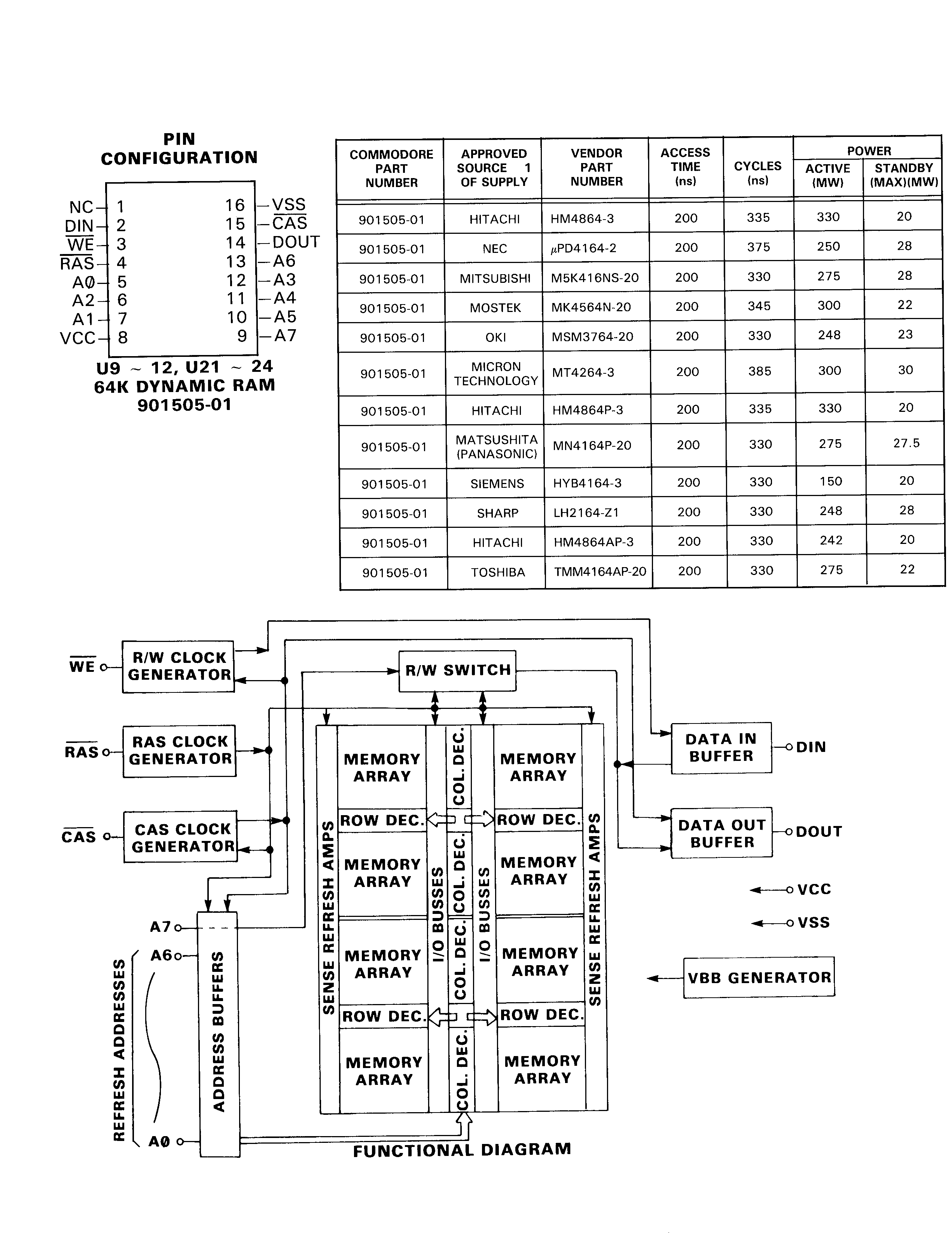
|
Section 1
NOTE: Most of the schematics listed here are relative large GIF Images (100 KB - 1 MB).
The scanned datasheets for the following chips
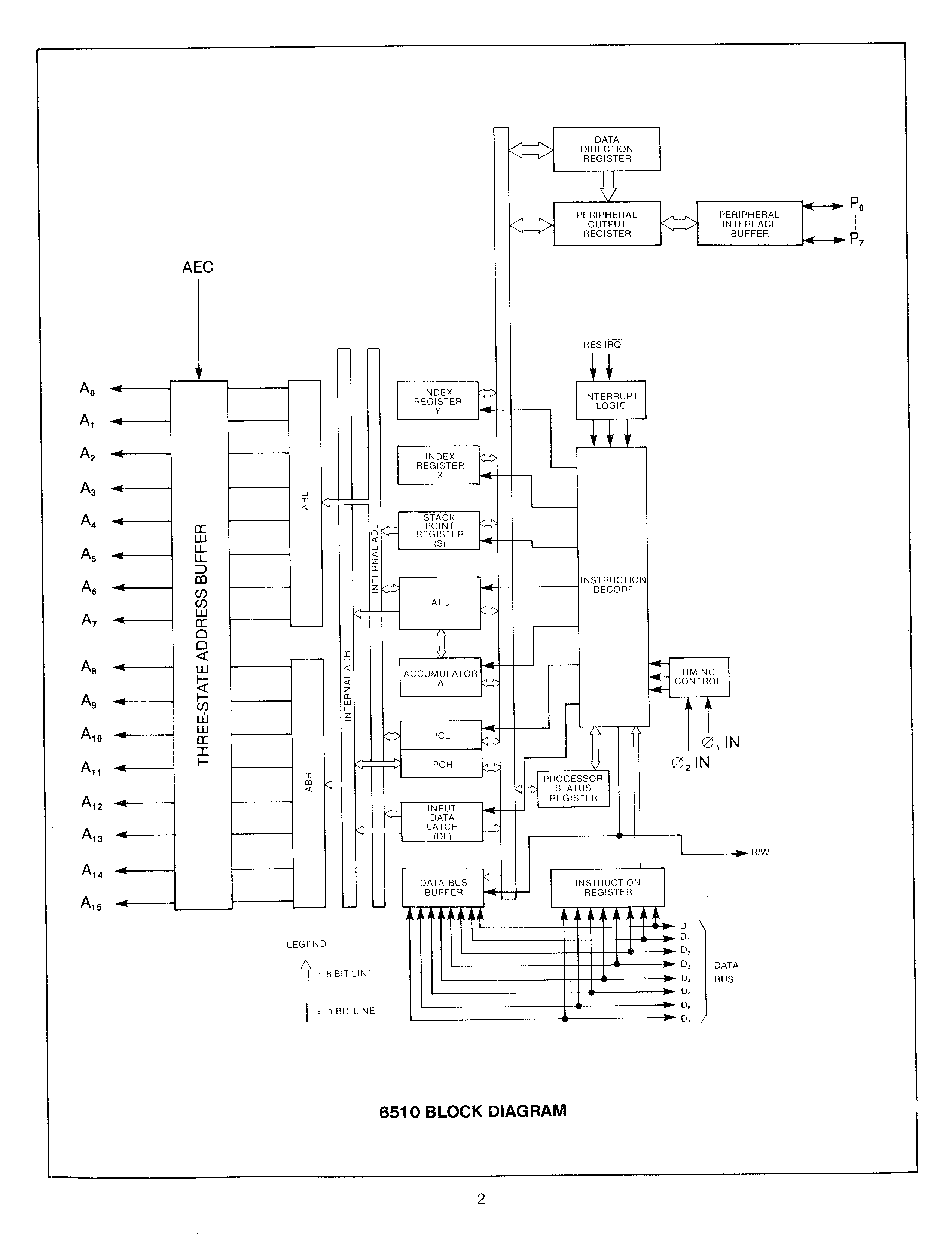
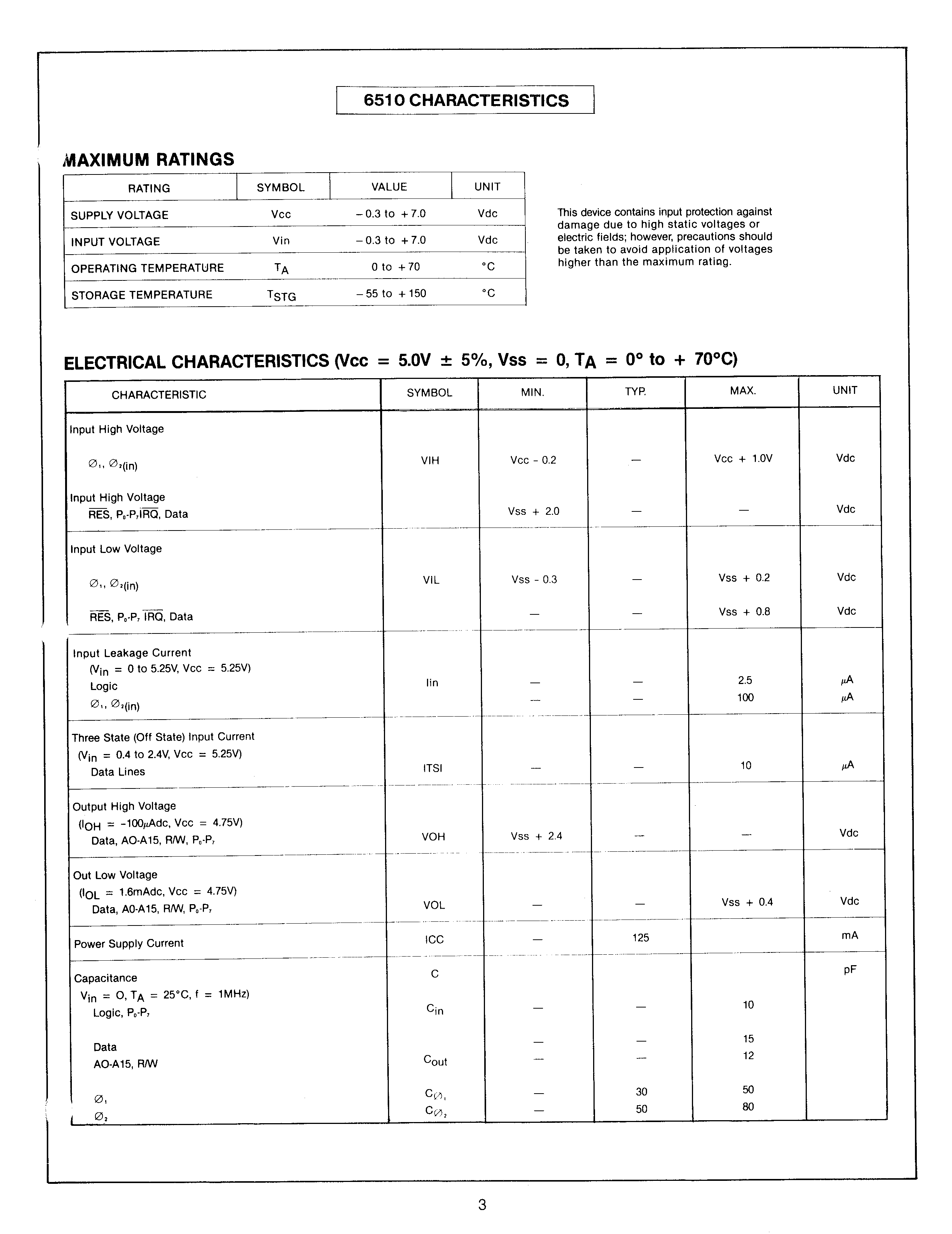
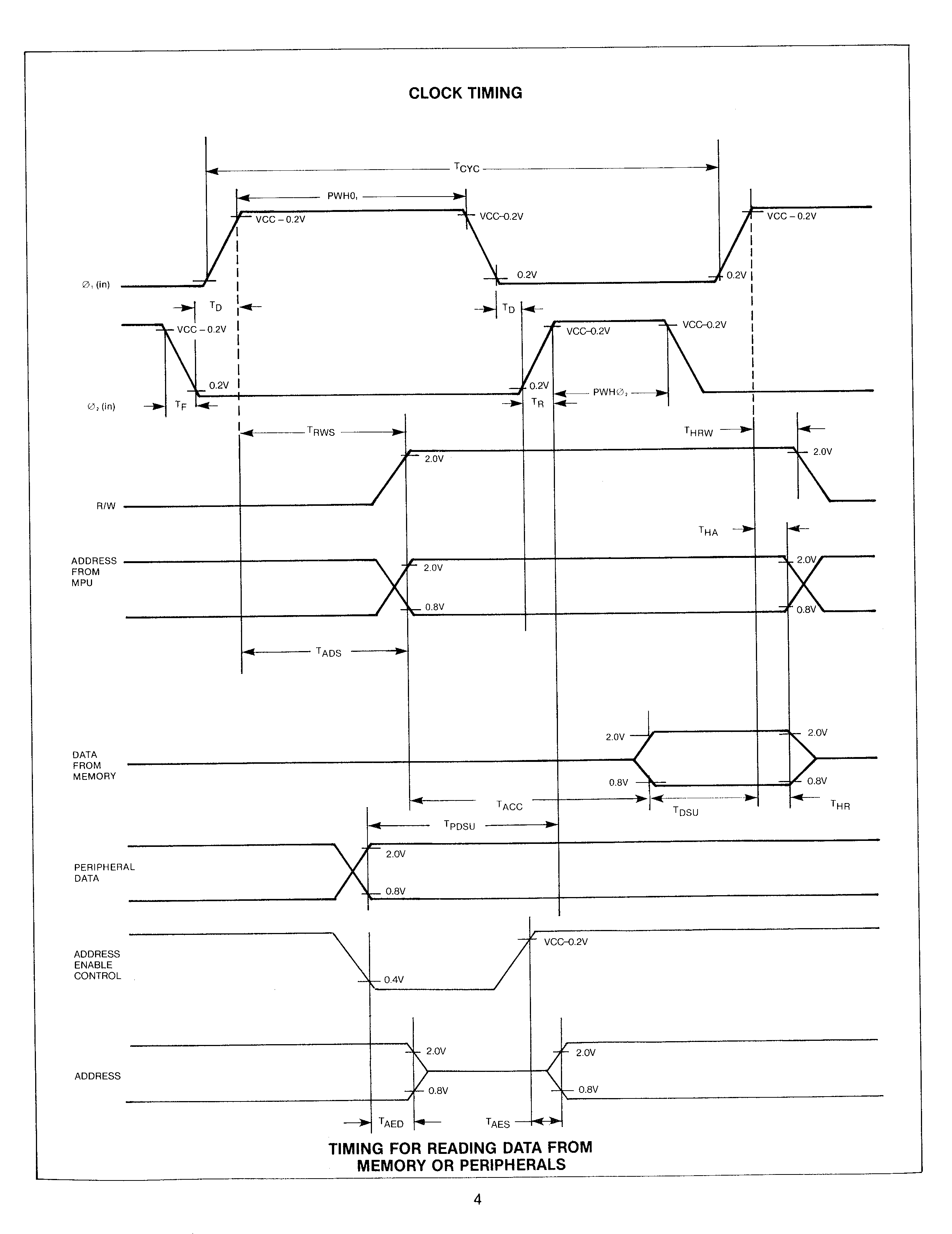
- 6510: page
01,
02,
03,
04,
05,
06,
07,
08,
09,
10
- 6522: page
01,
02,
03,
04,
05,
06,
07,
08,
09,
10,
11,
12,
13,
14,
15,
16,
17,
18,
19,
20,
21,
22,
23,
24
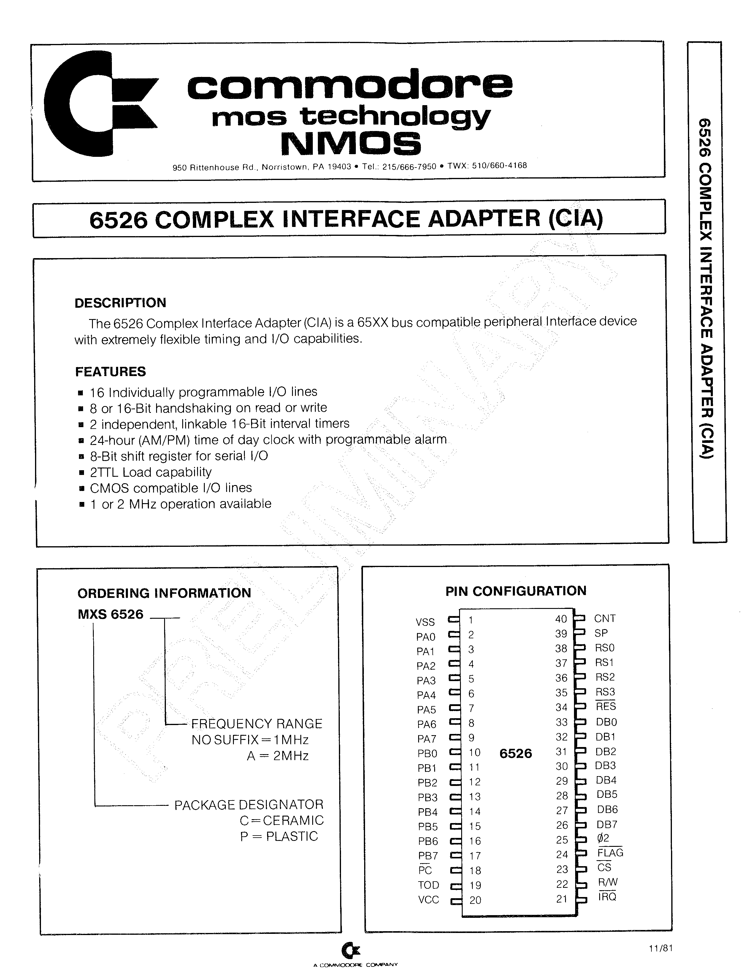
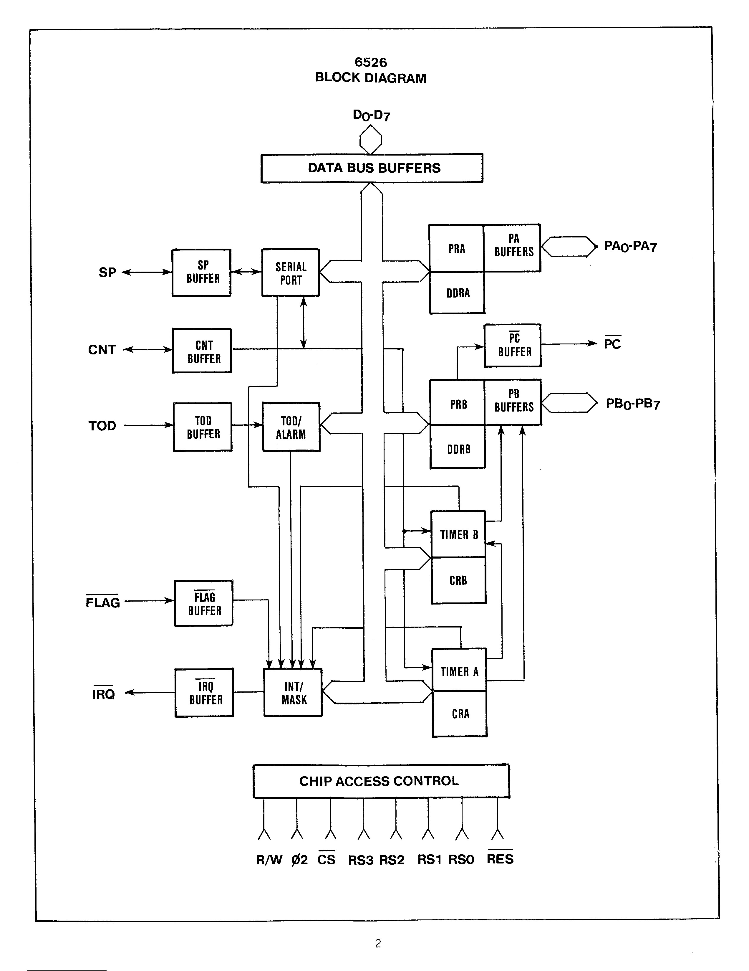
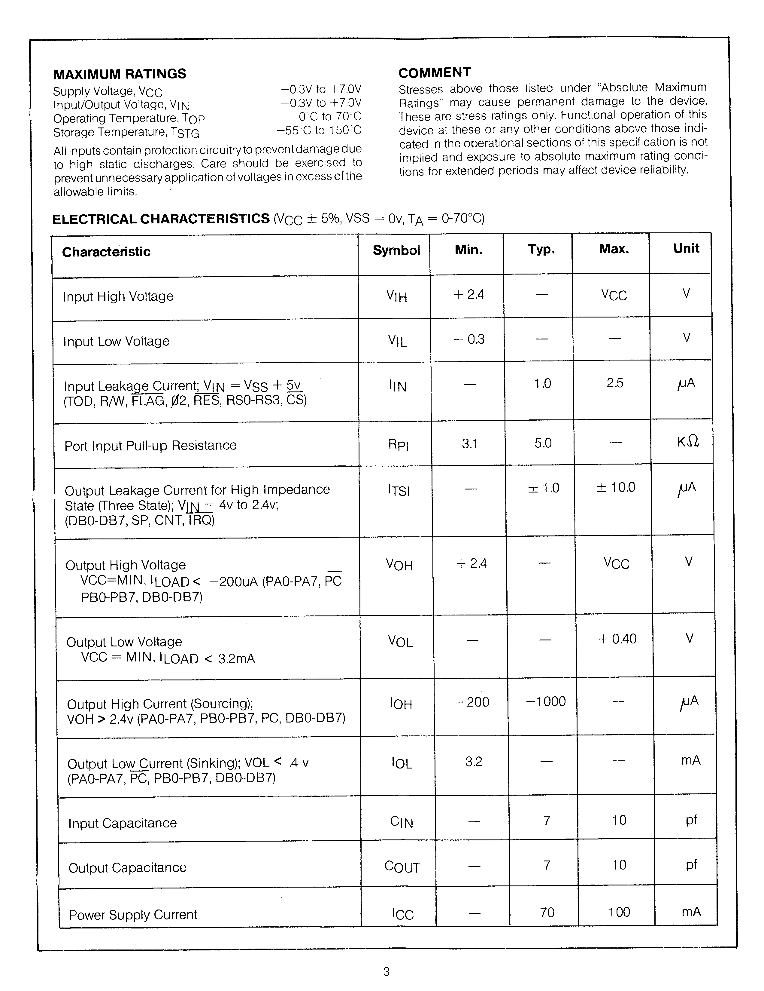
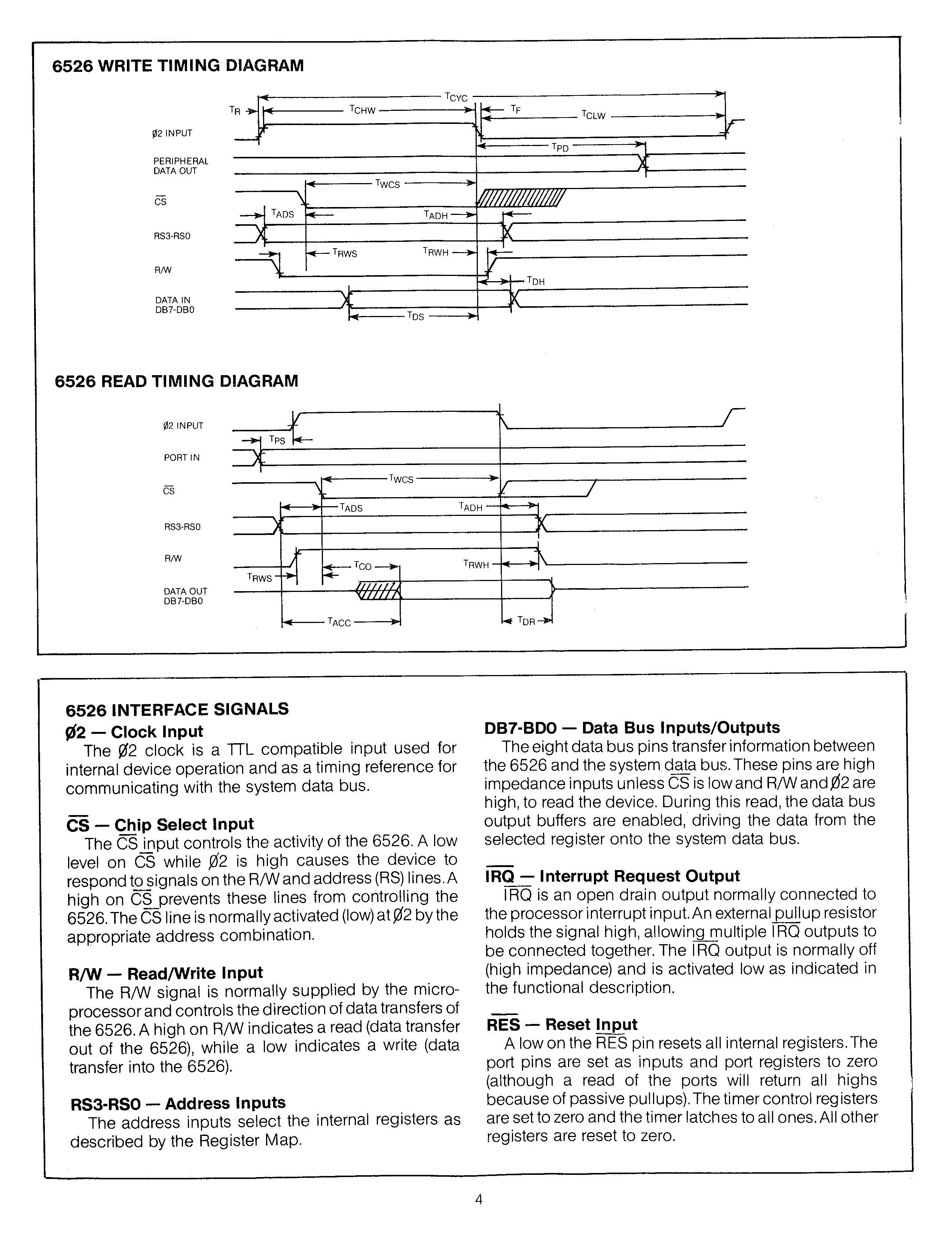
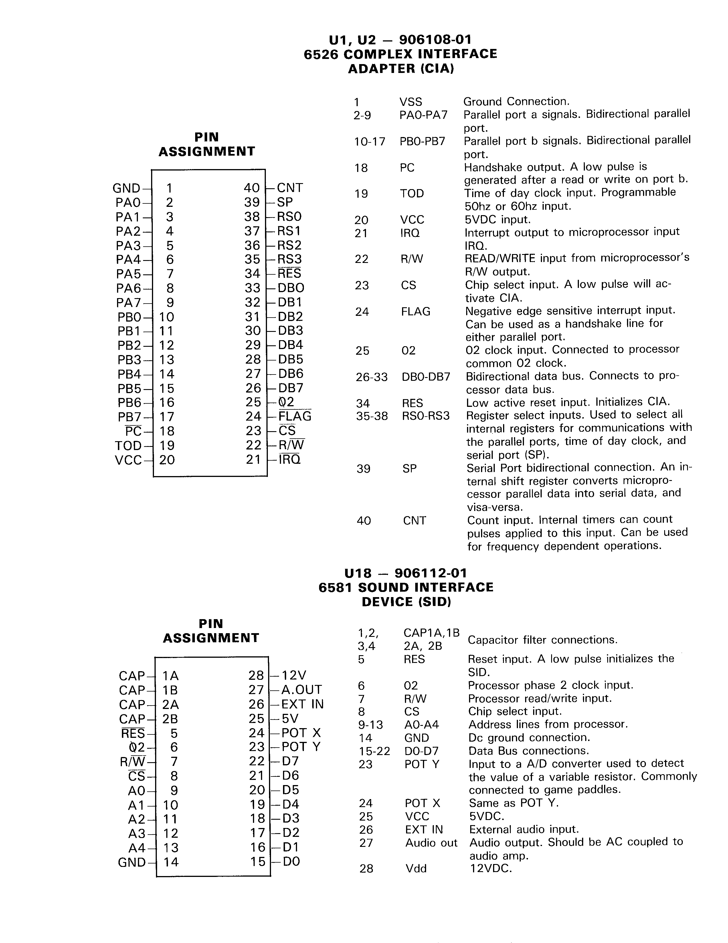
- 6526: page
01,
02,
03,
04,
05,
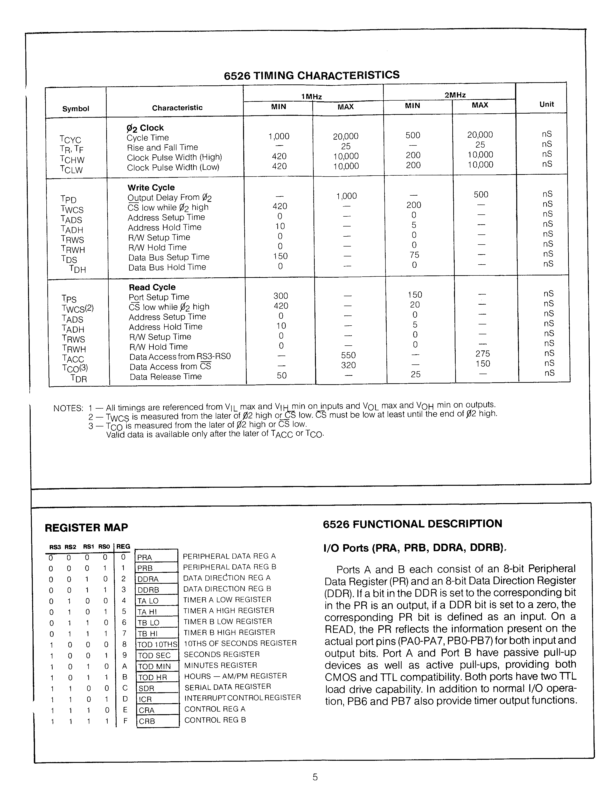
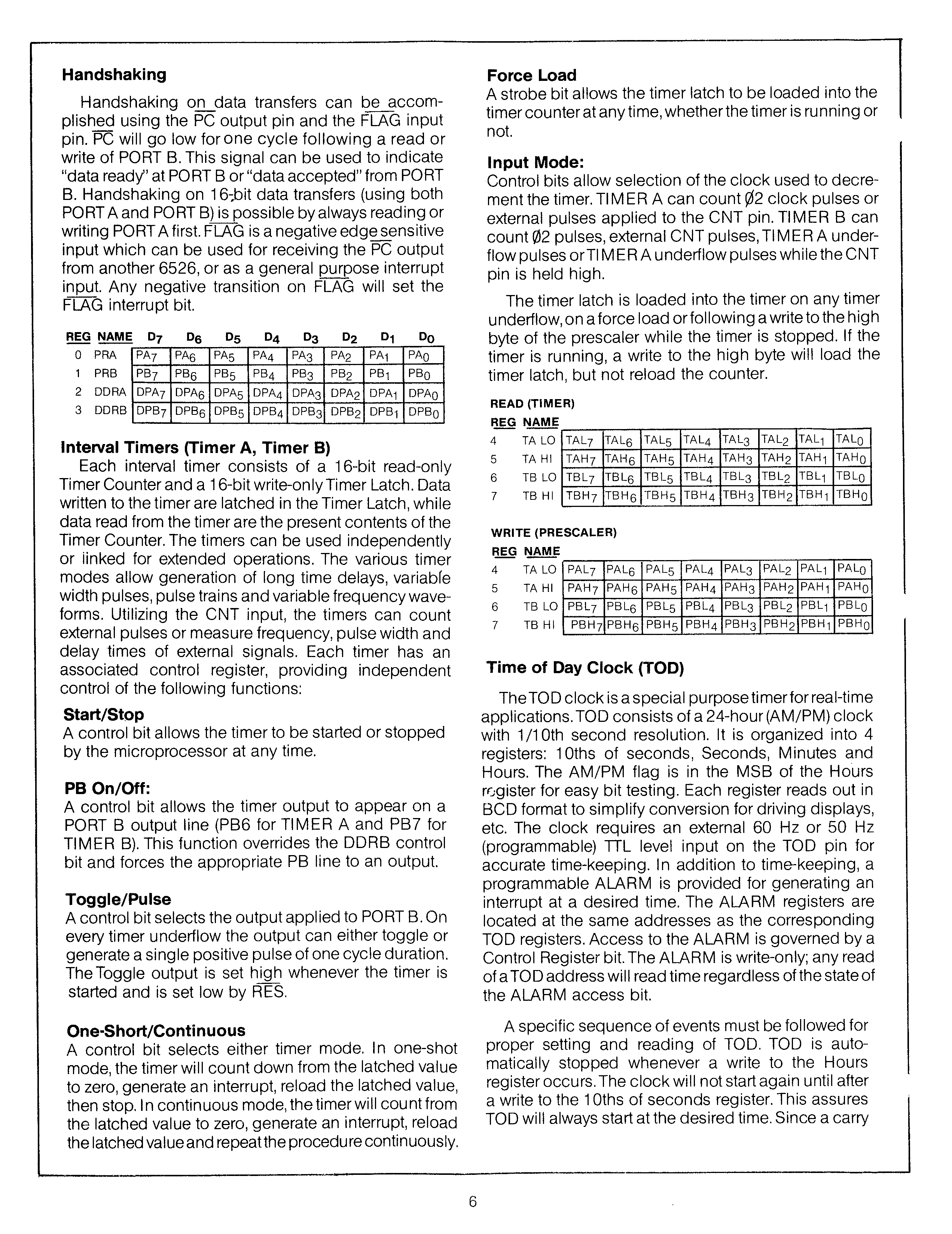
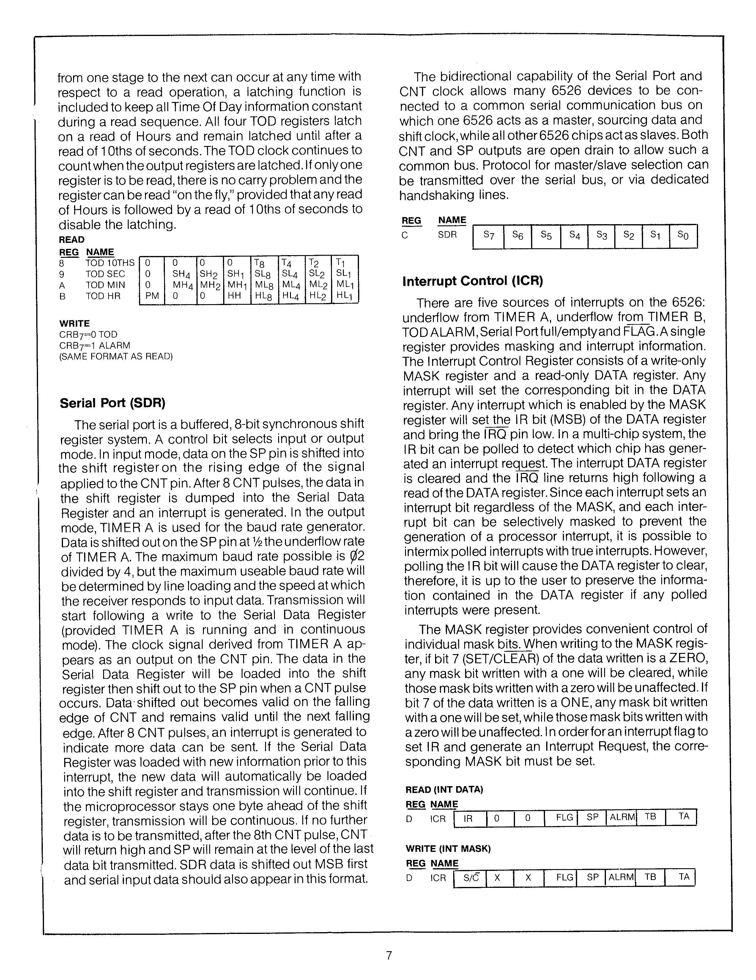
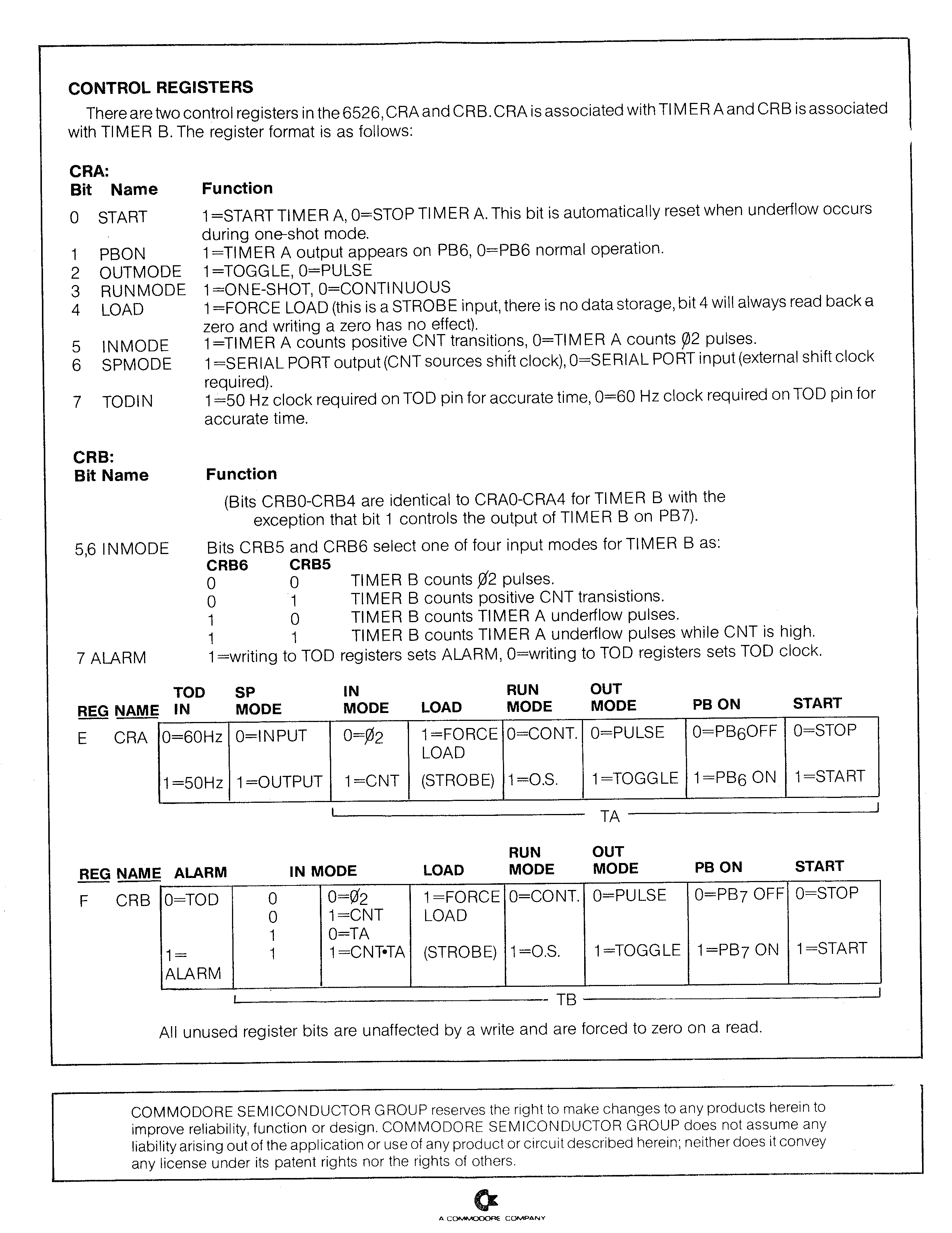
06,
07,
08
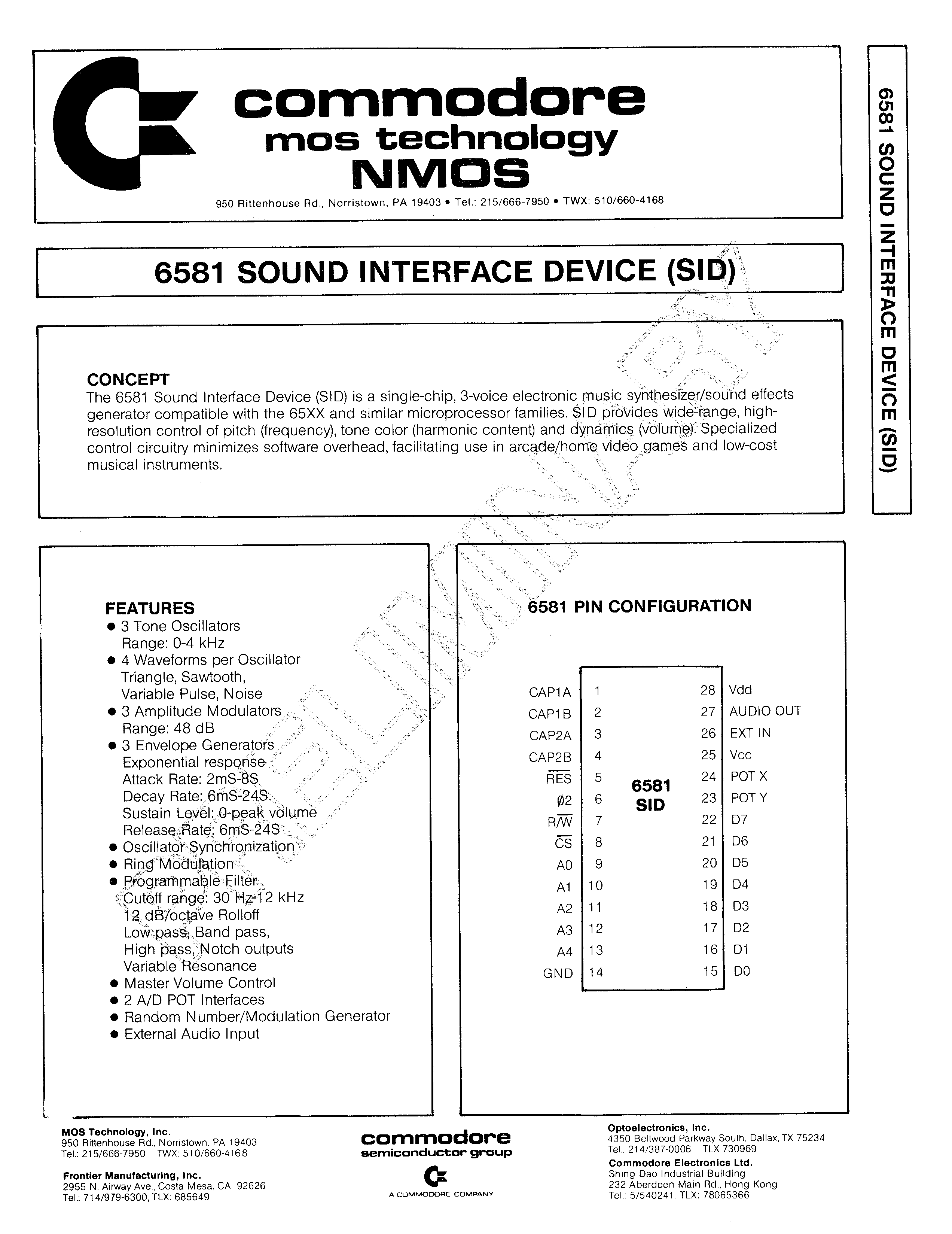
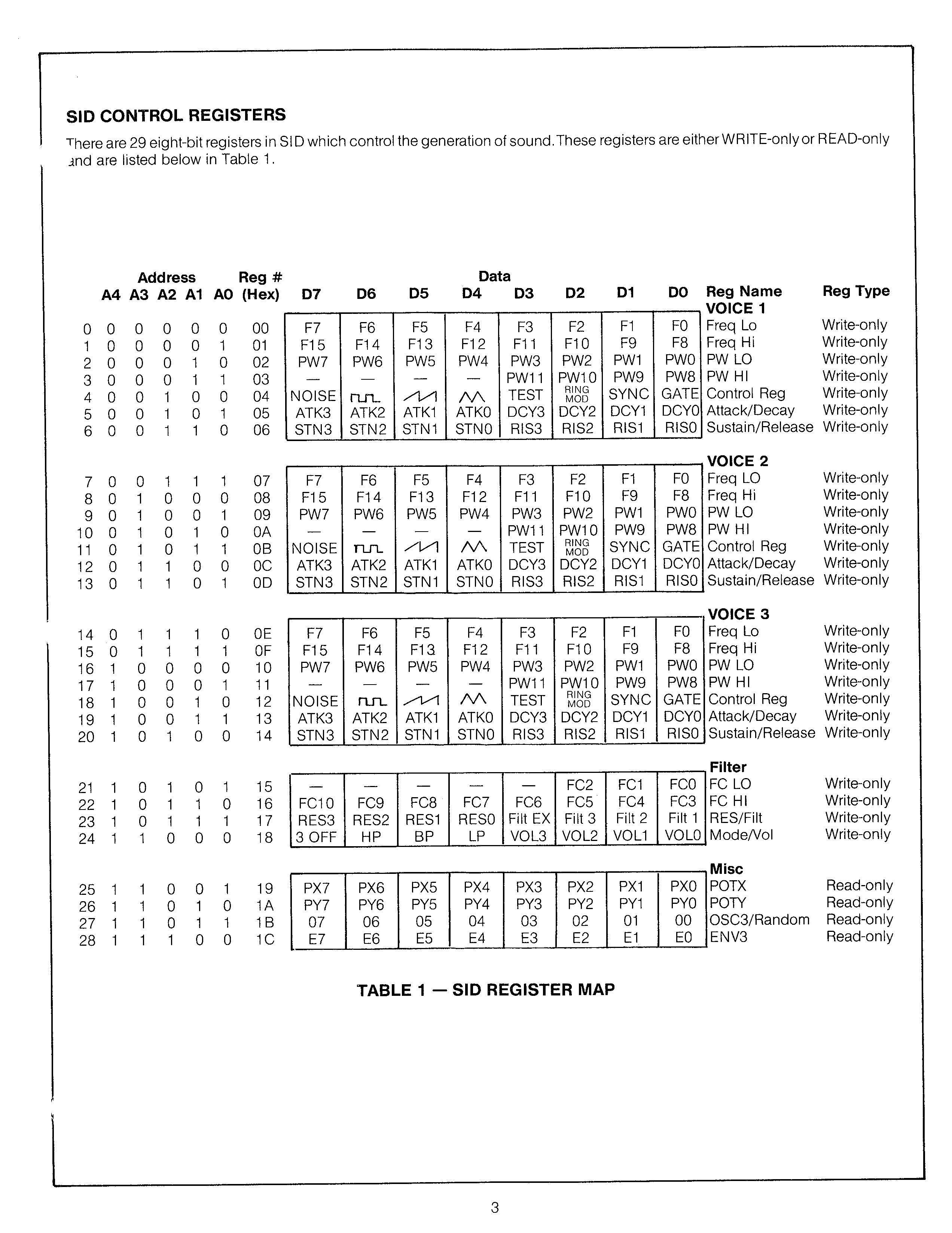
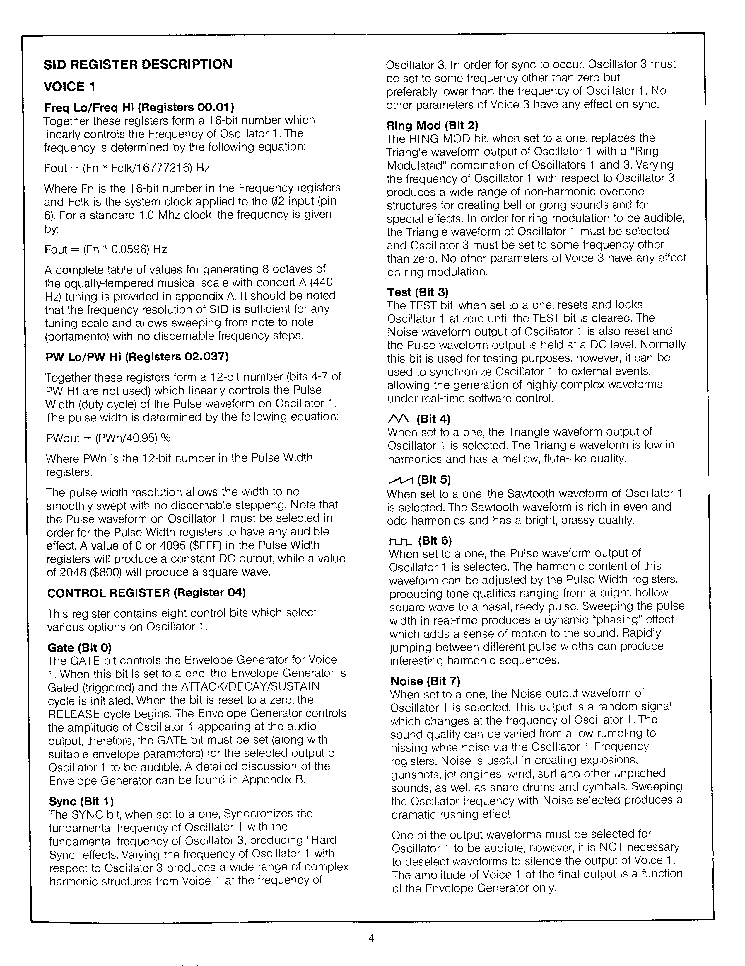
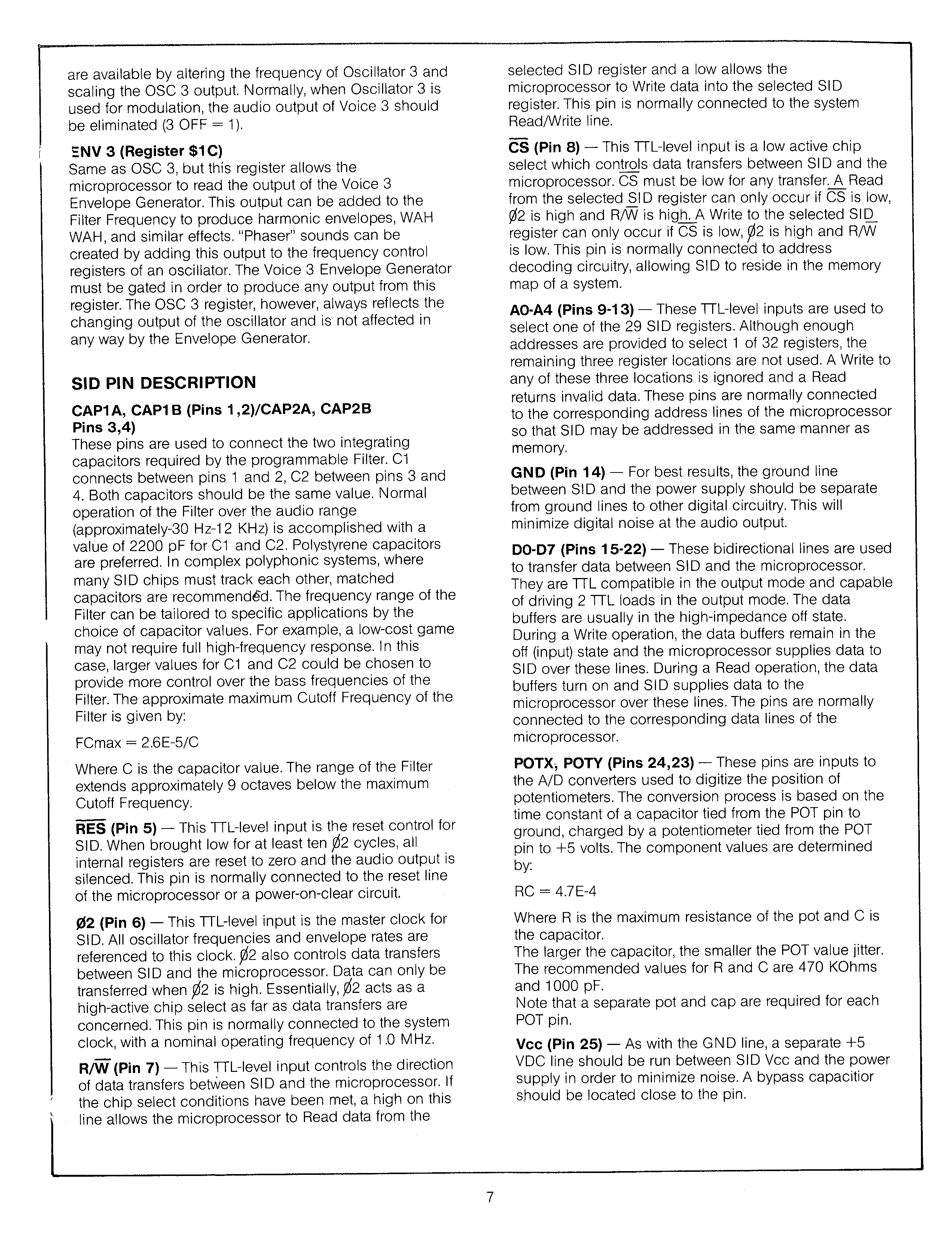
- 6581: page
01,
02,
03,
04,
05,
06,
07,
08,
09,
10,
11,
12
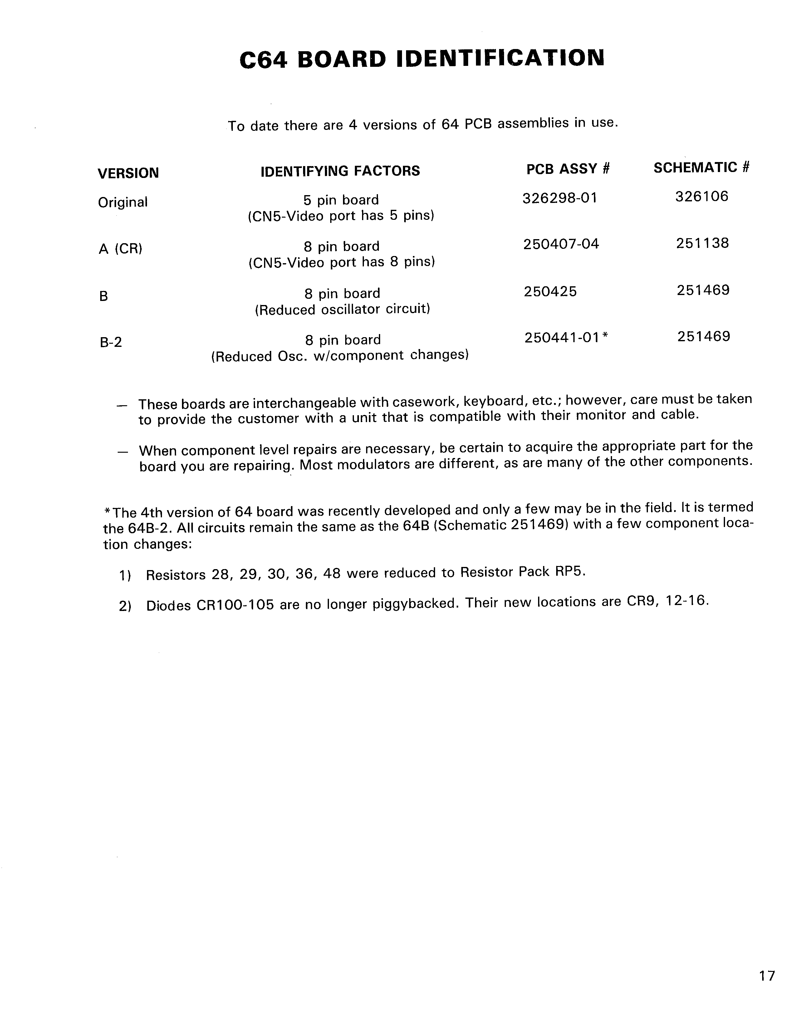
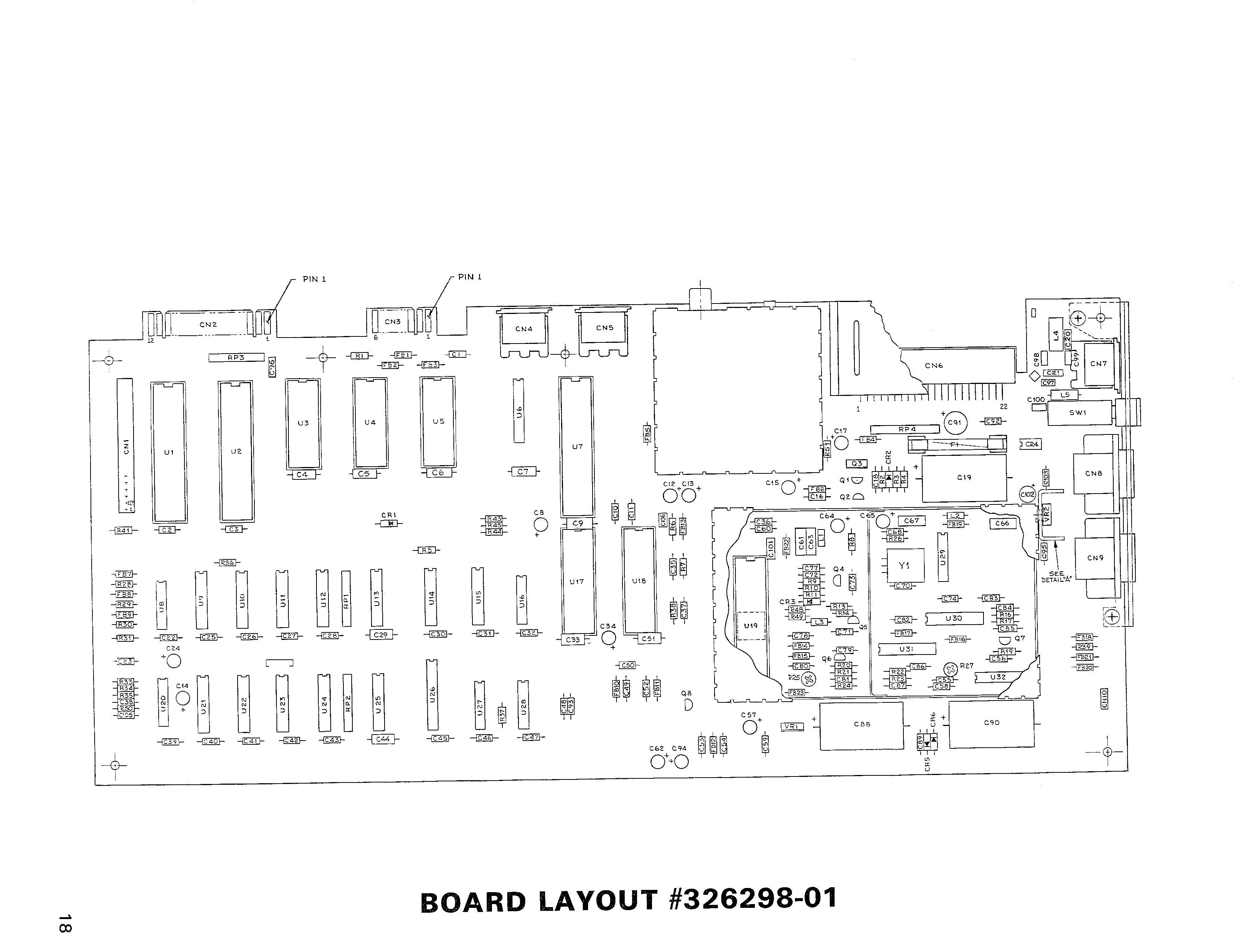
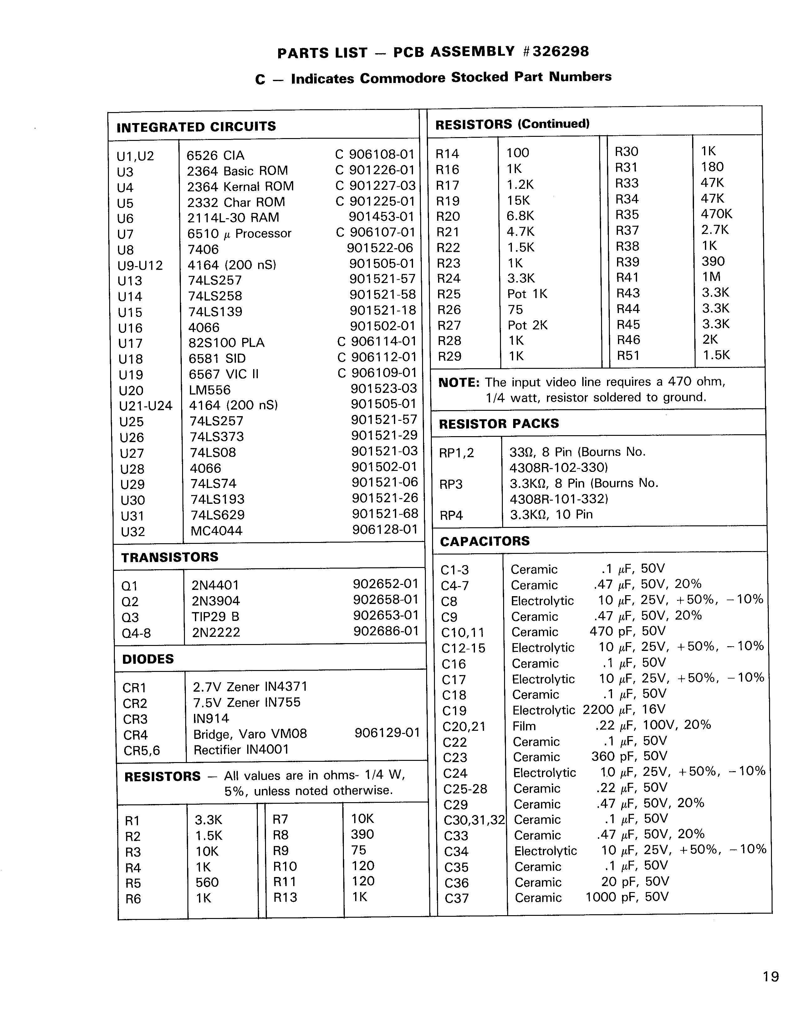
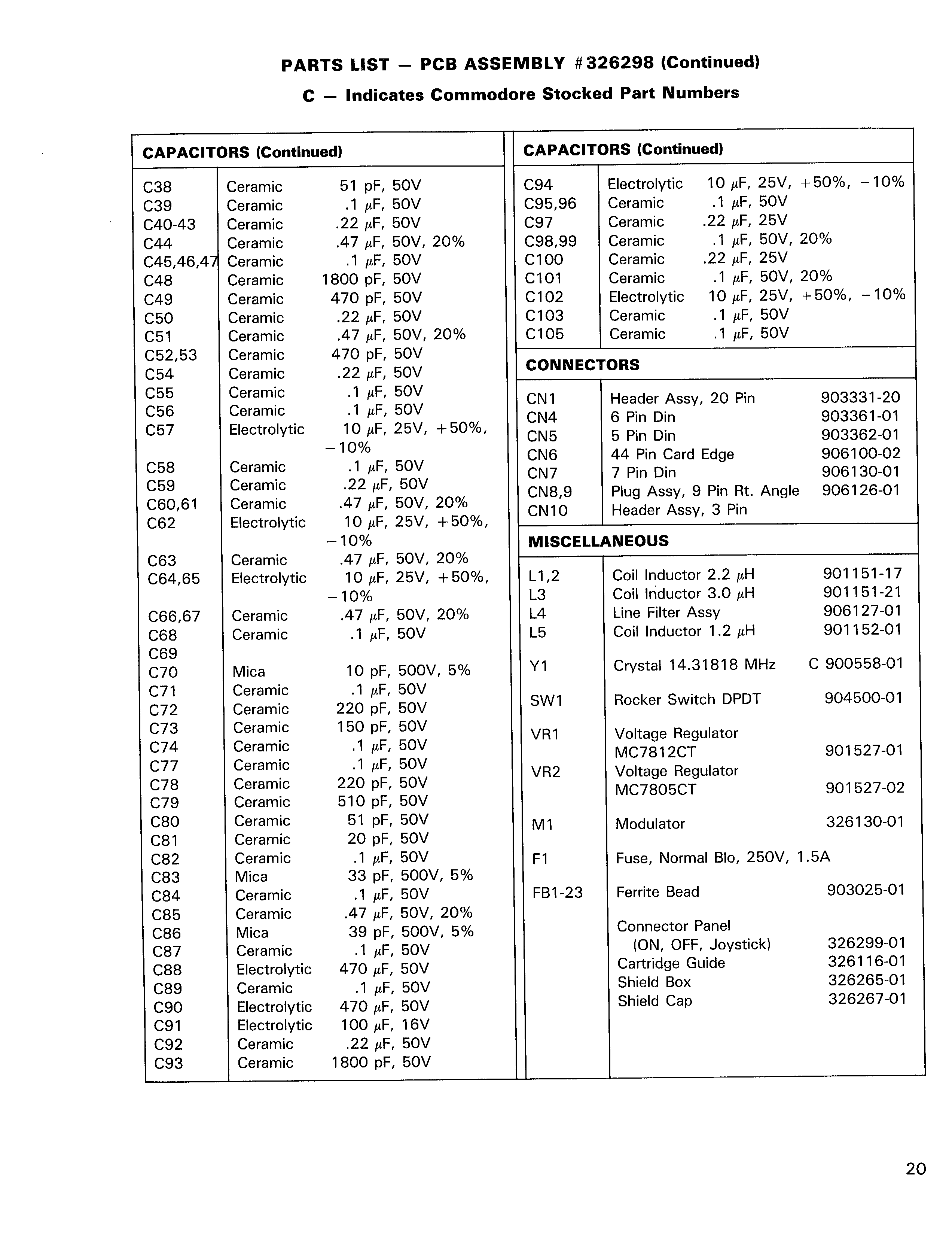
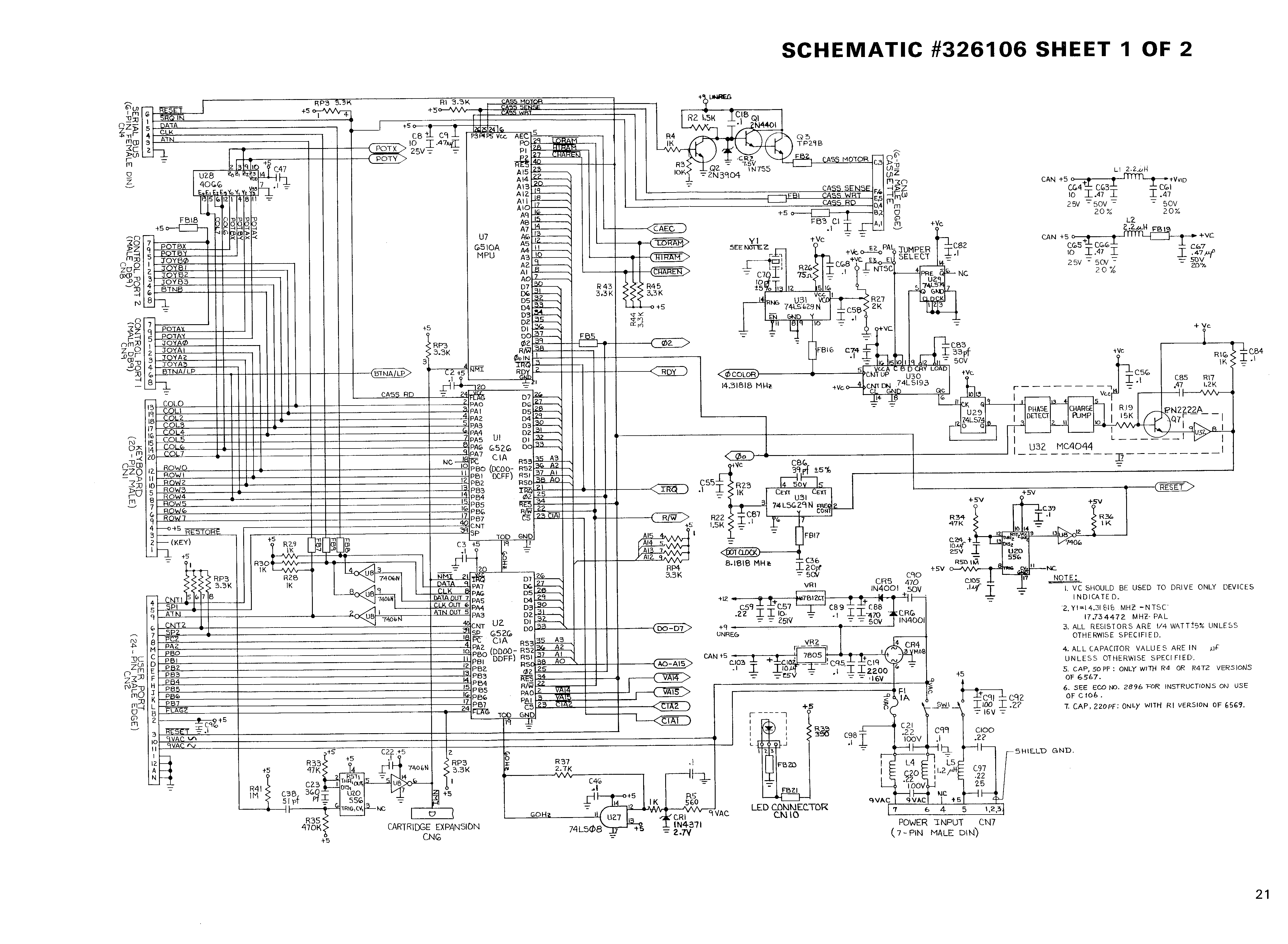
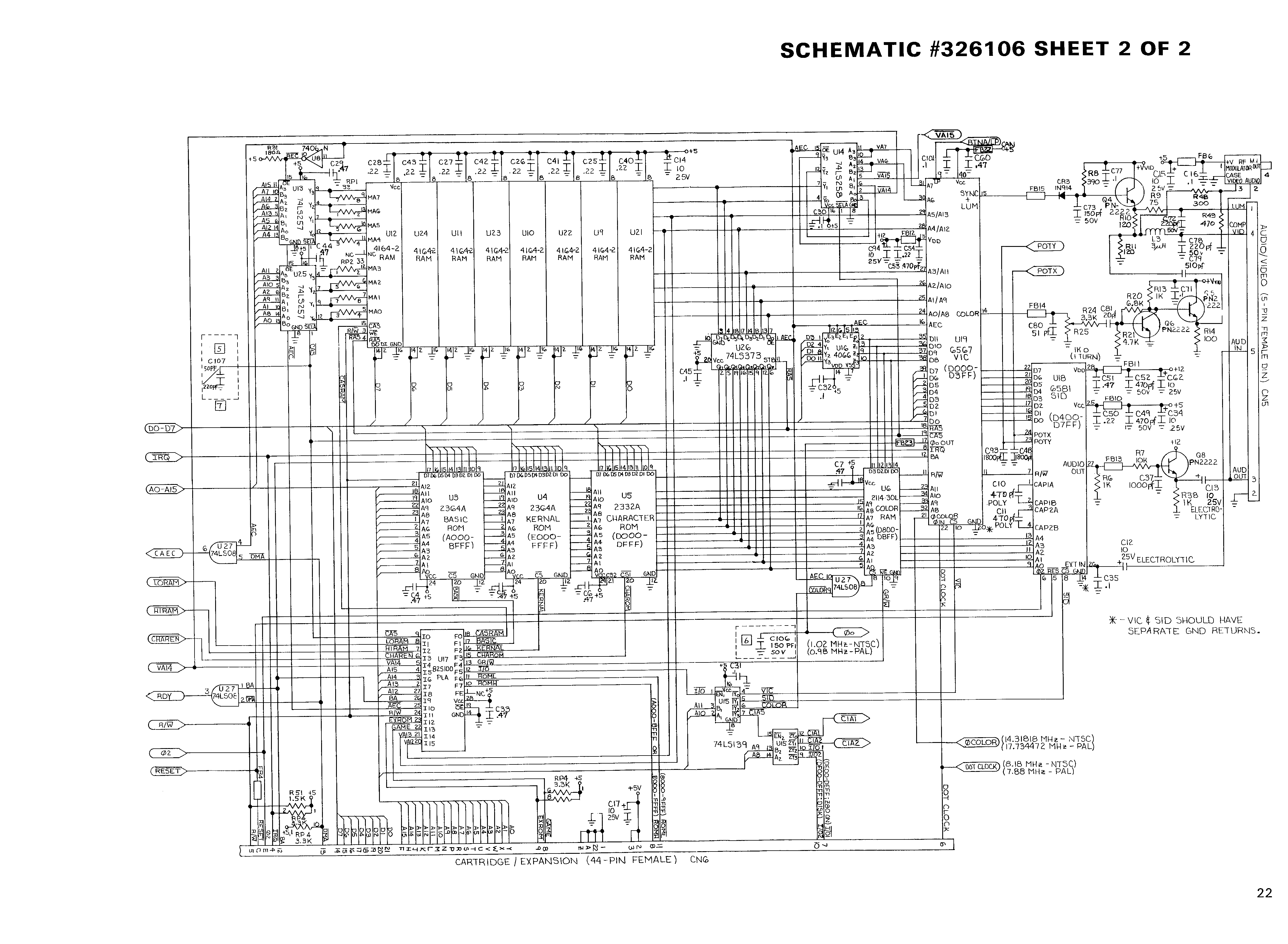
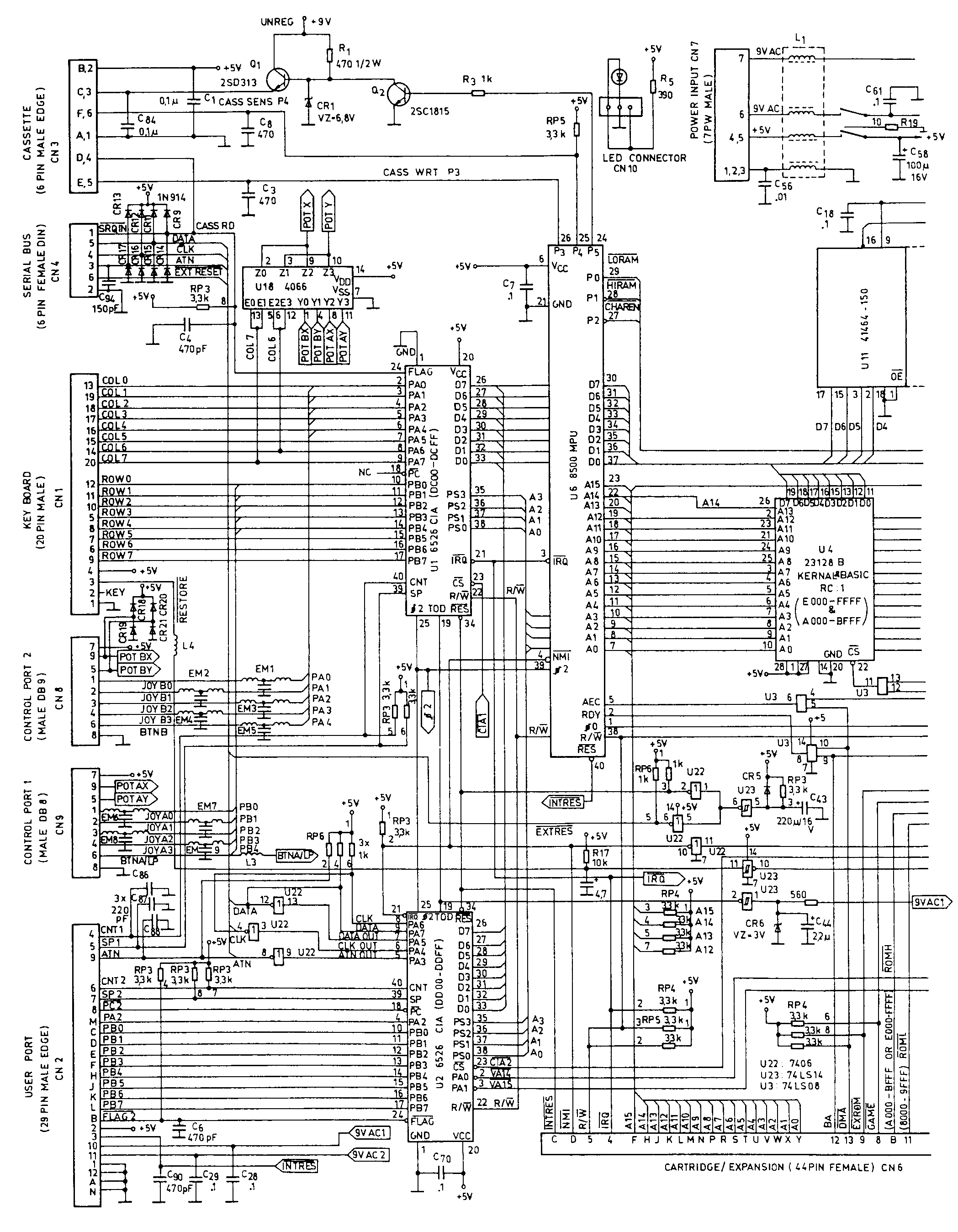
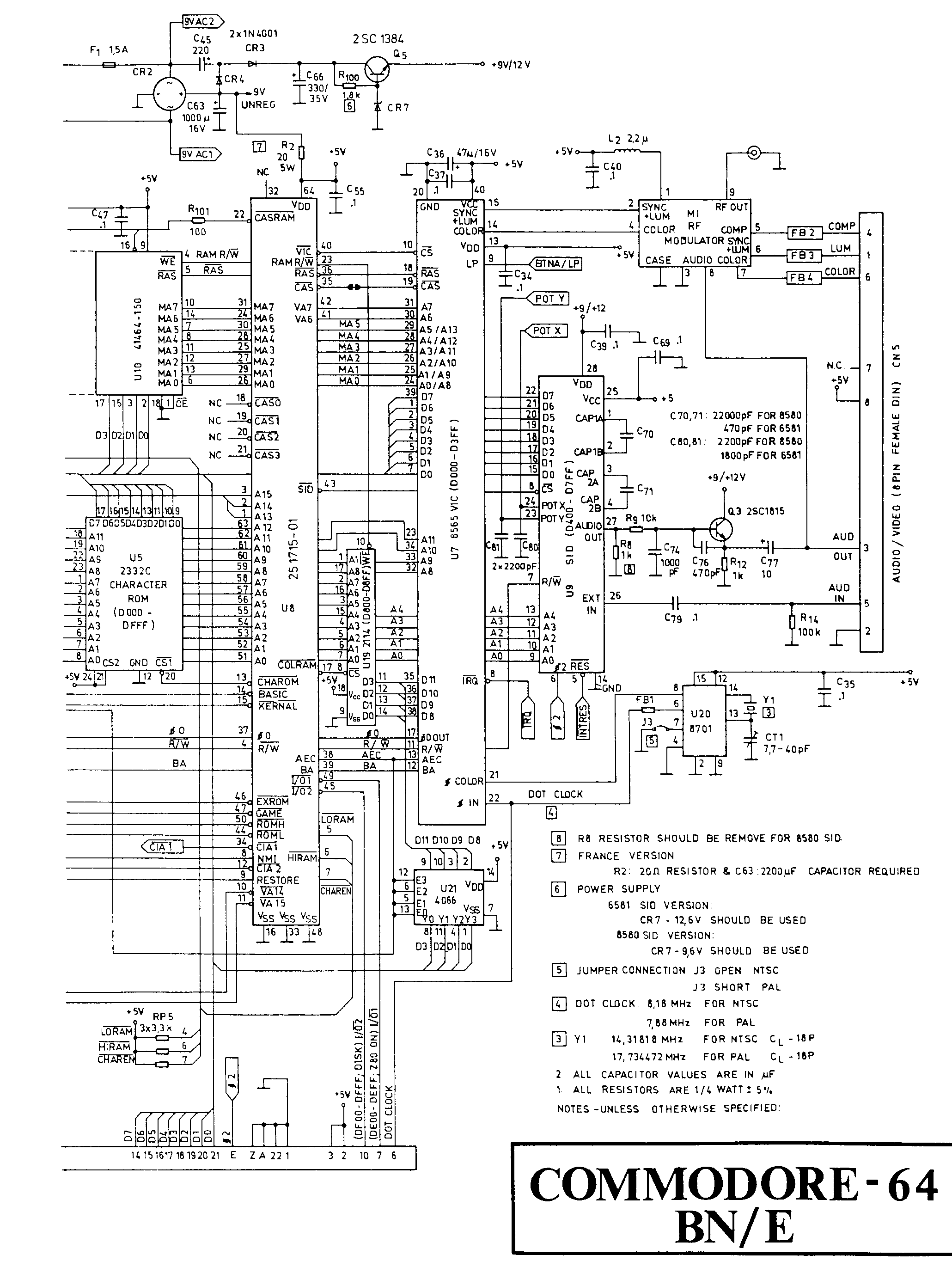
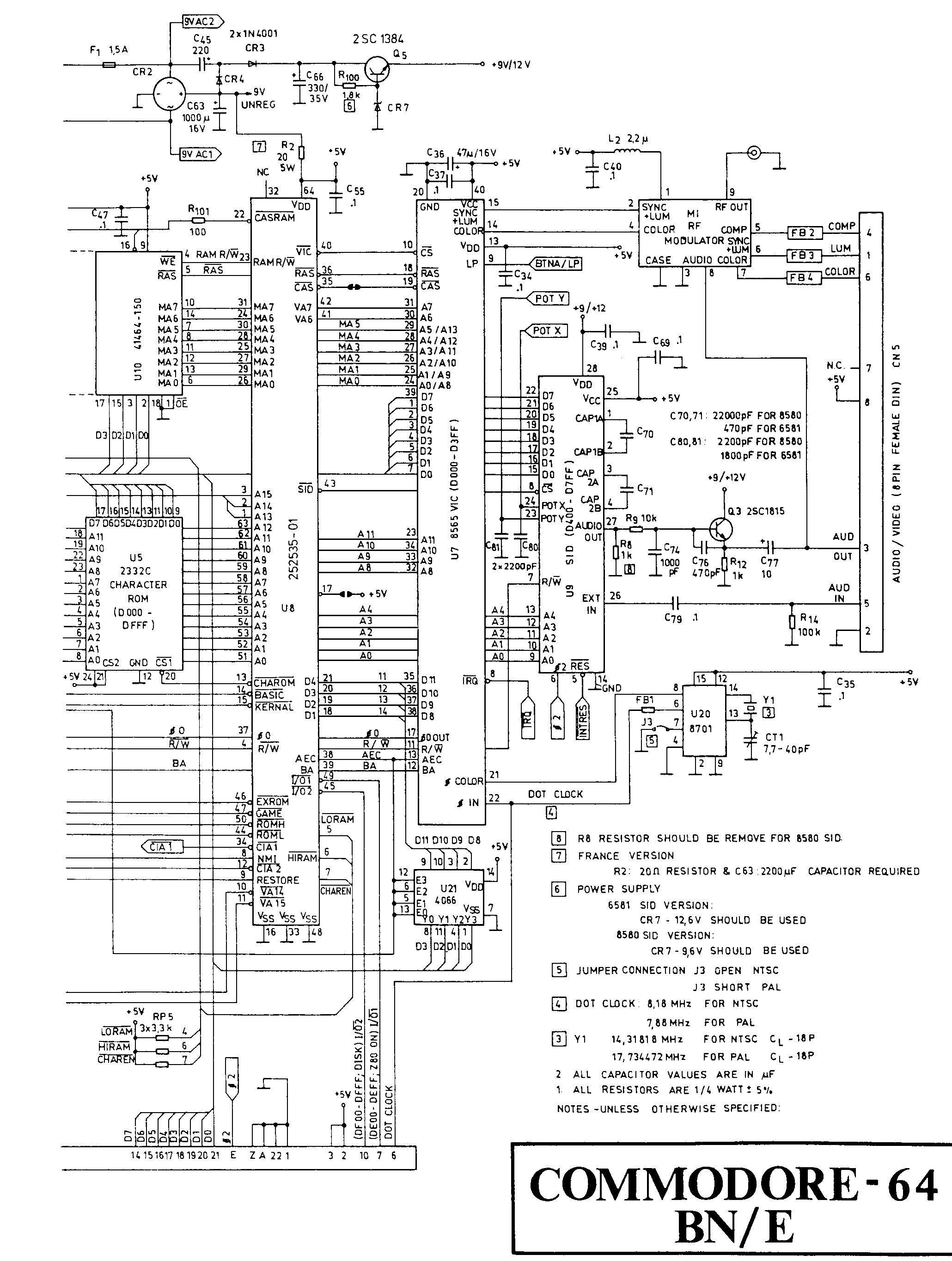
The scanned C64 Service Manual from 1985 (with detailed wiring diagrams)
- page:
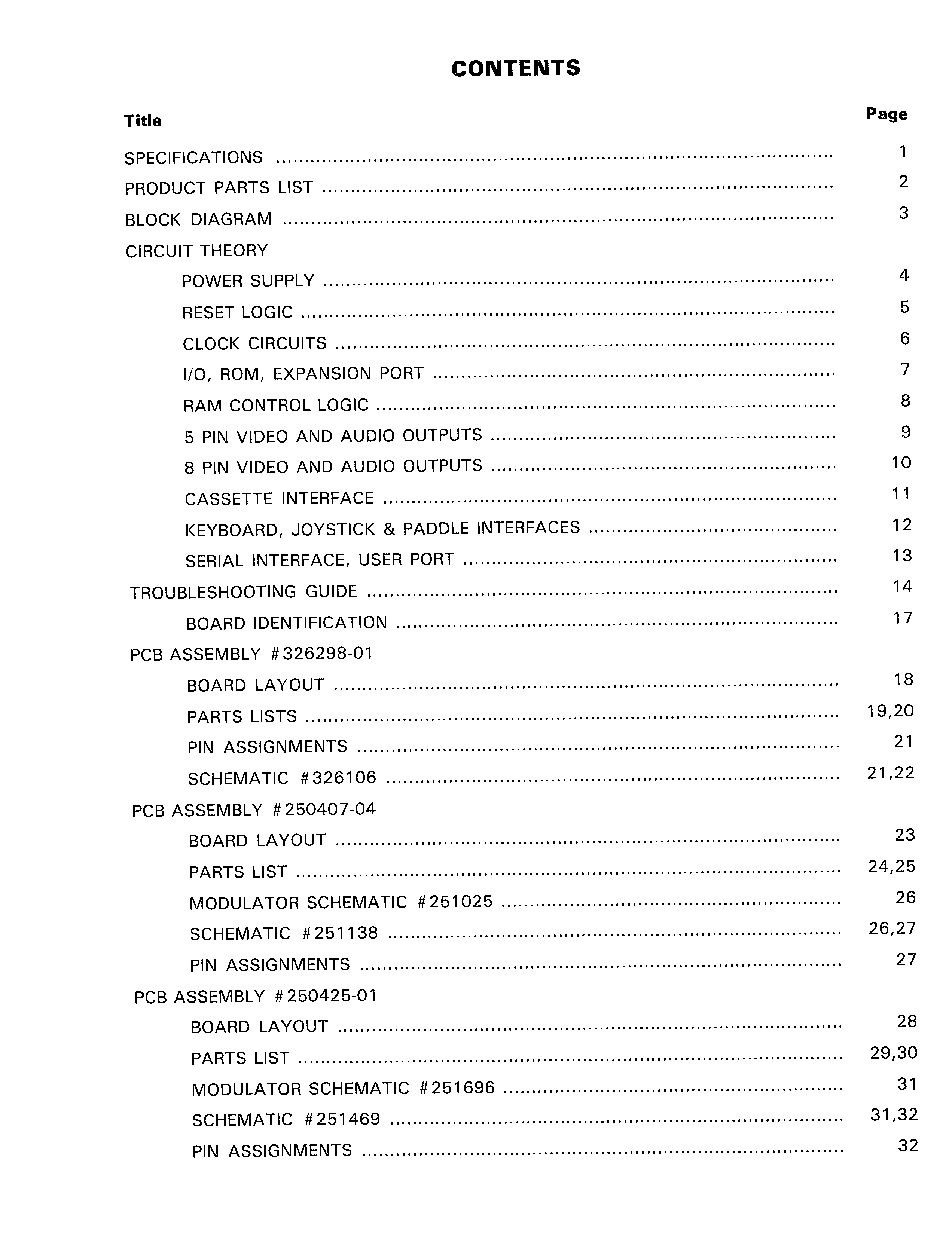
title,
contents,
01,
02,
03,
04,
05,
06,
07,
08,
09,
10,
11,
12,
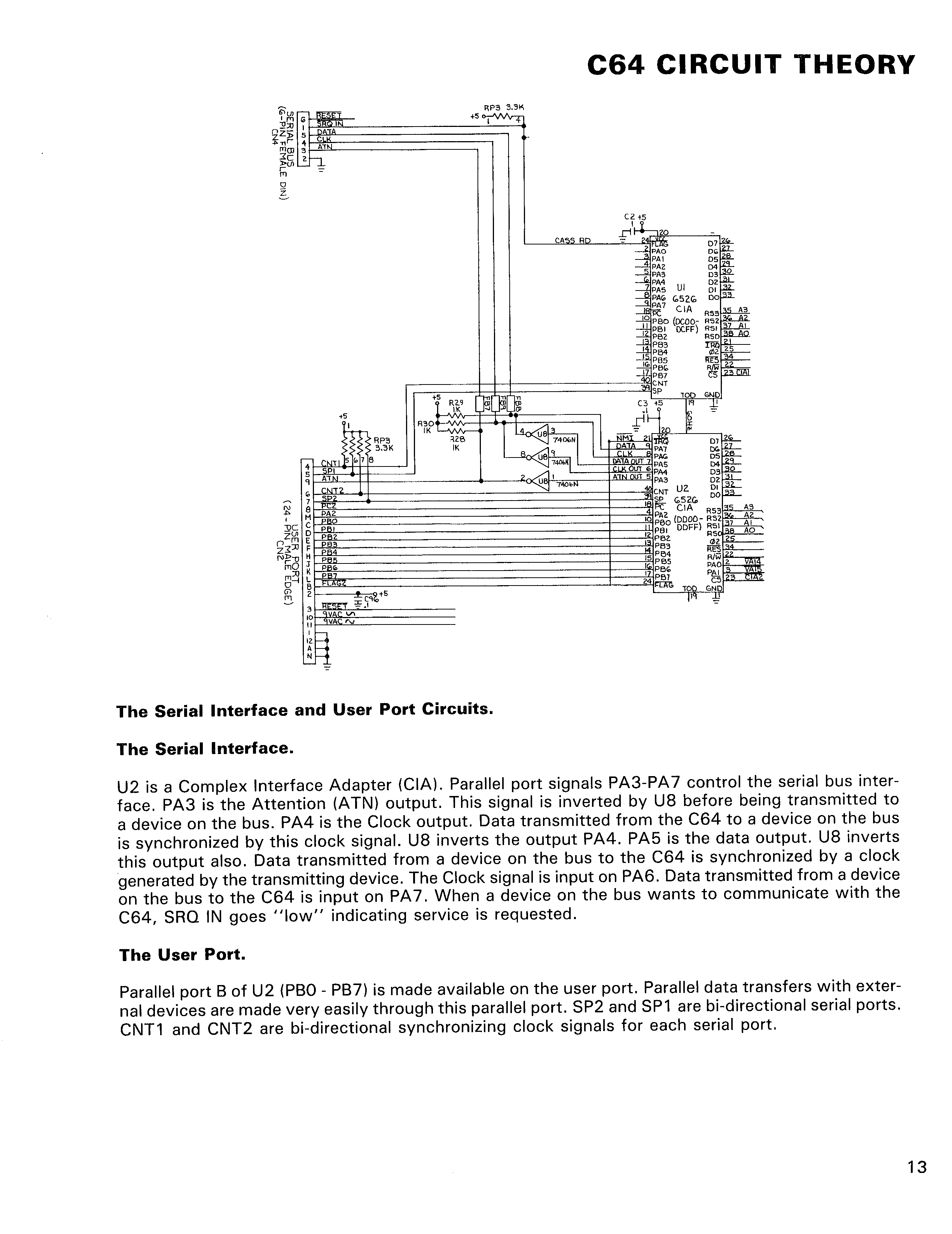
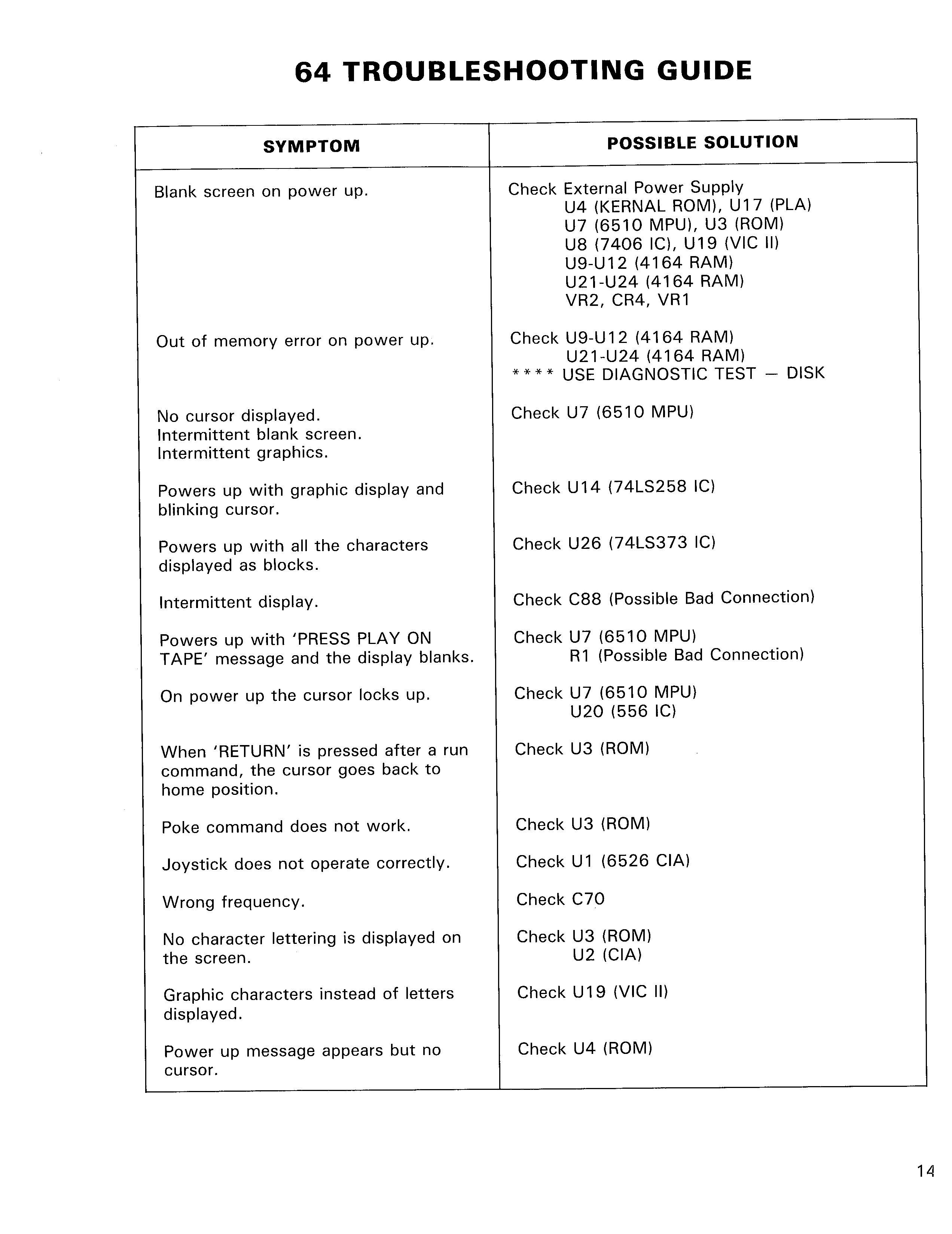
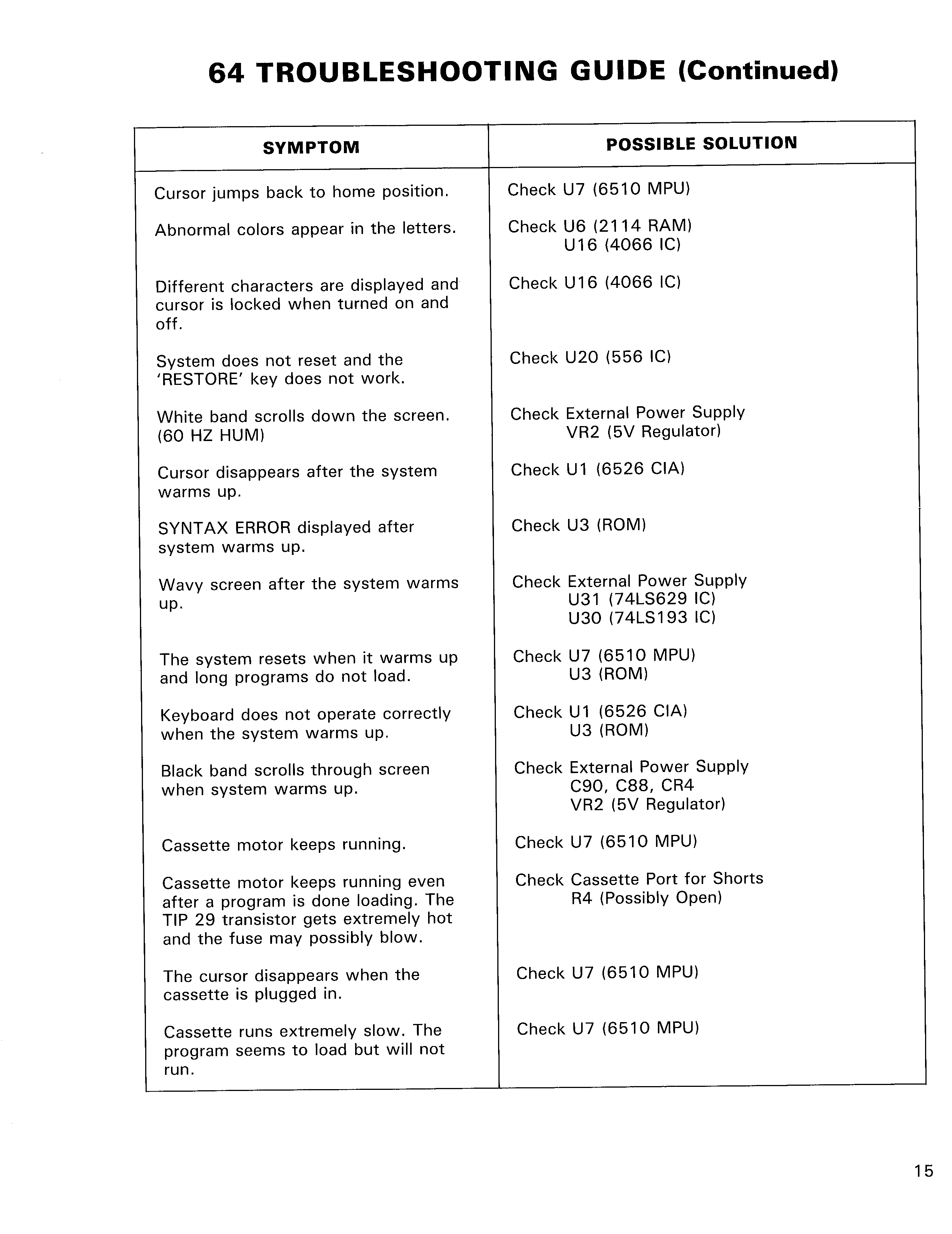
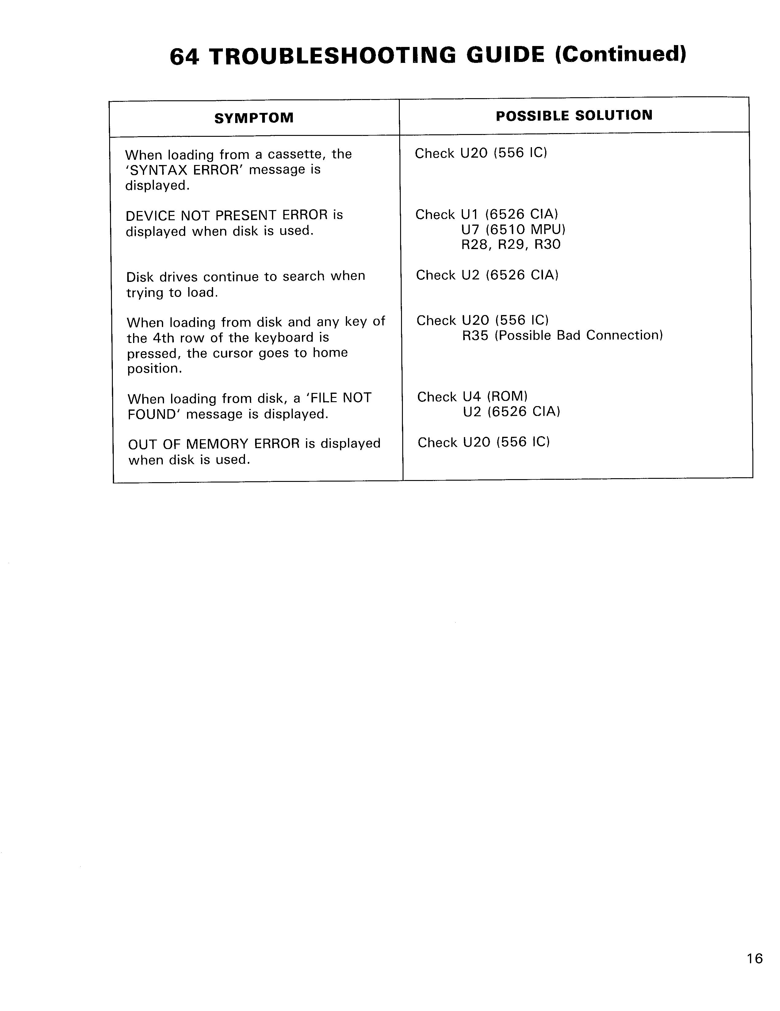
13,
14,
15,
16,
17,
18,
19,
20,
21a,
21b,
22a,
22b,
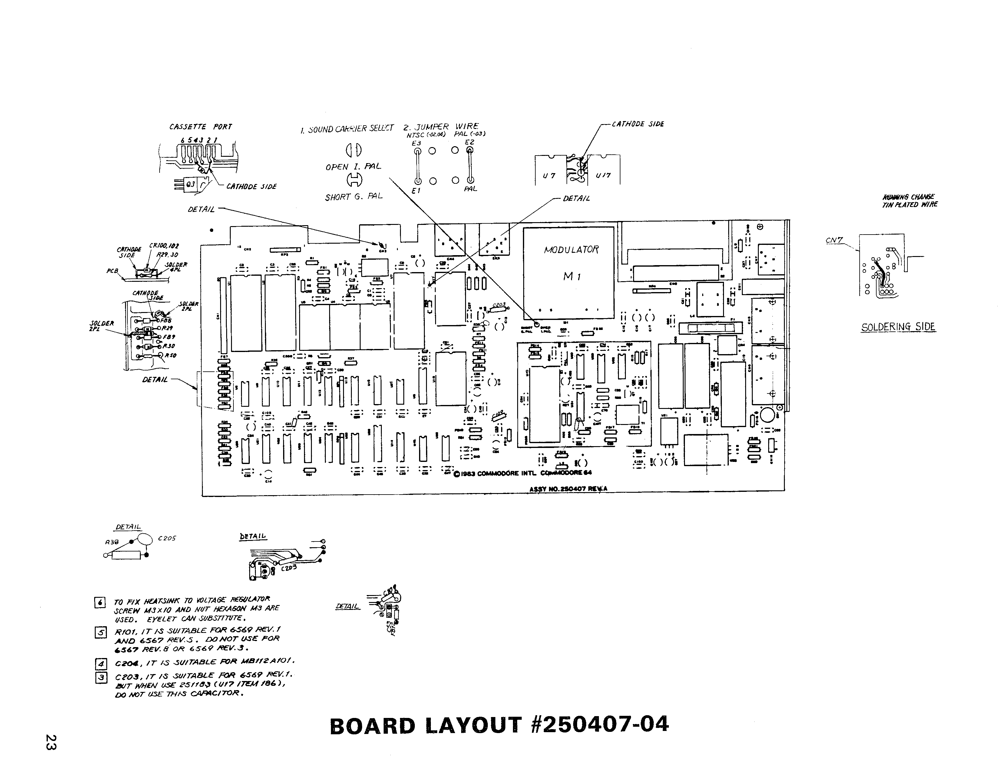
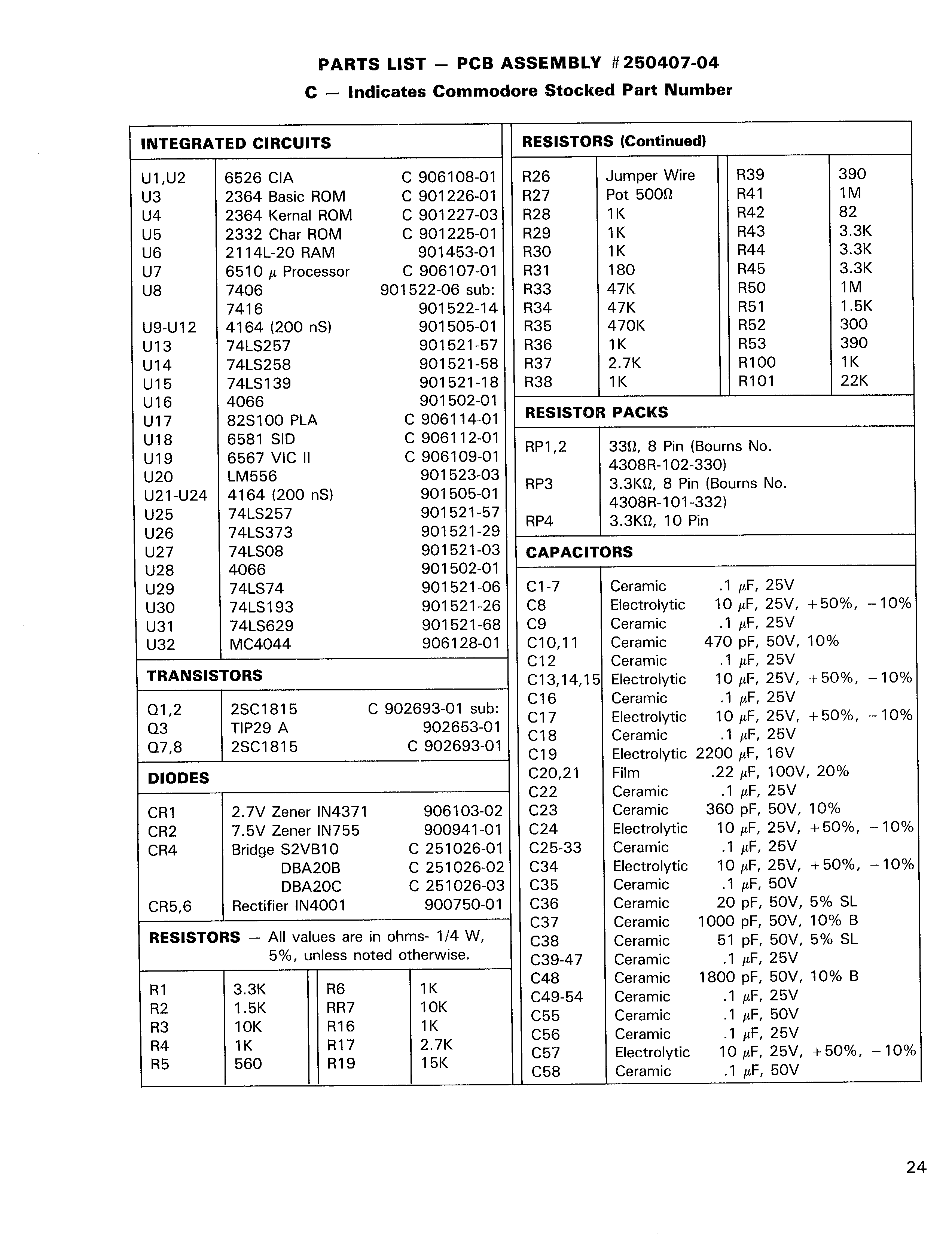
23,
24,
25,
26a,
26b,
27a,
27b,
28,
29,
30,
31a,
31b,
32a,
32b
The C64 Service Manual from 1985 in html format
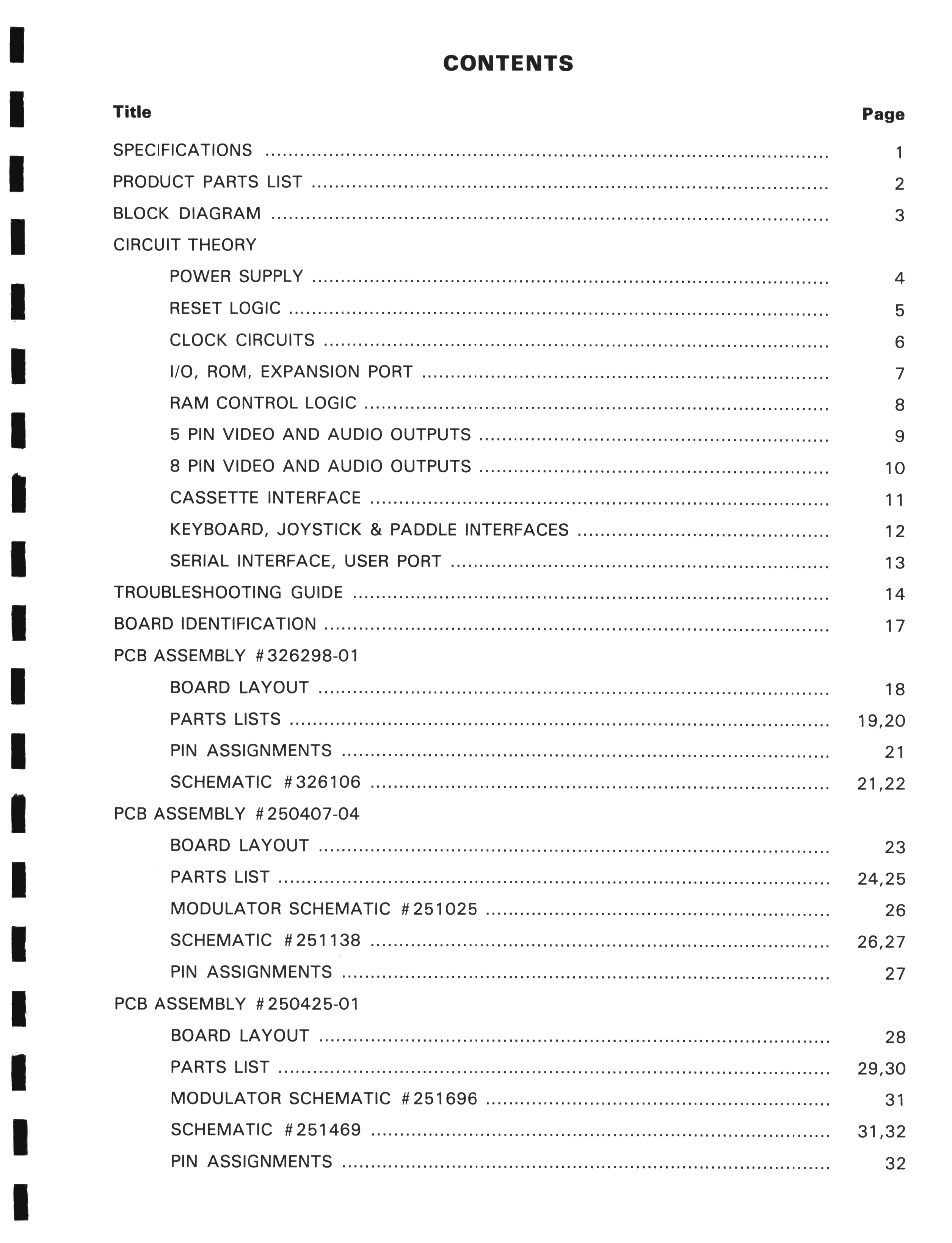
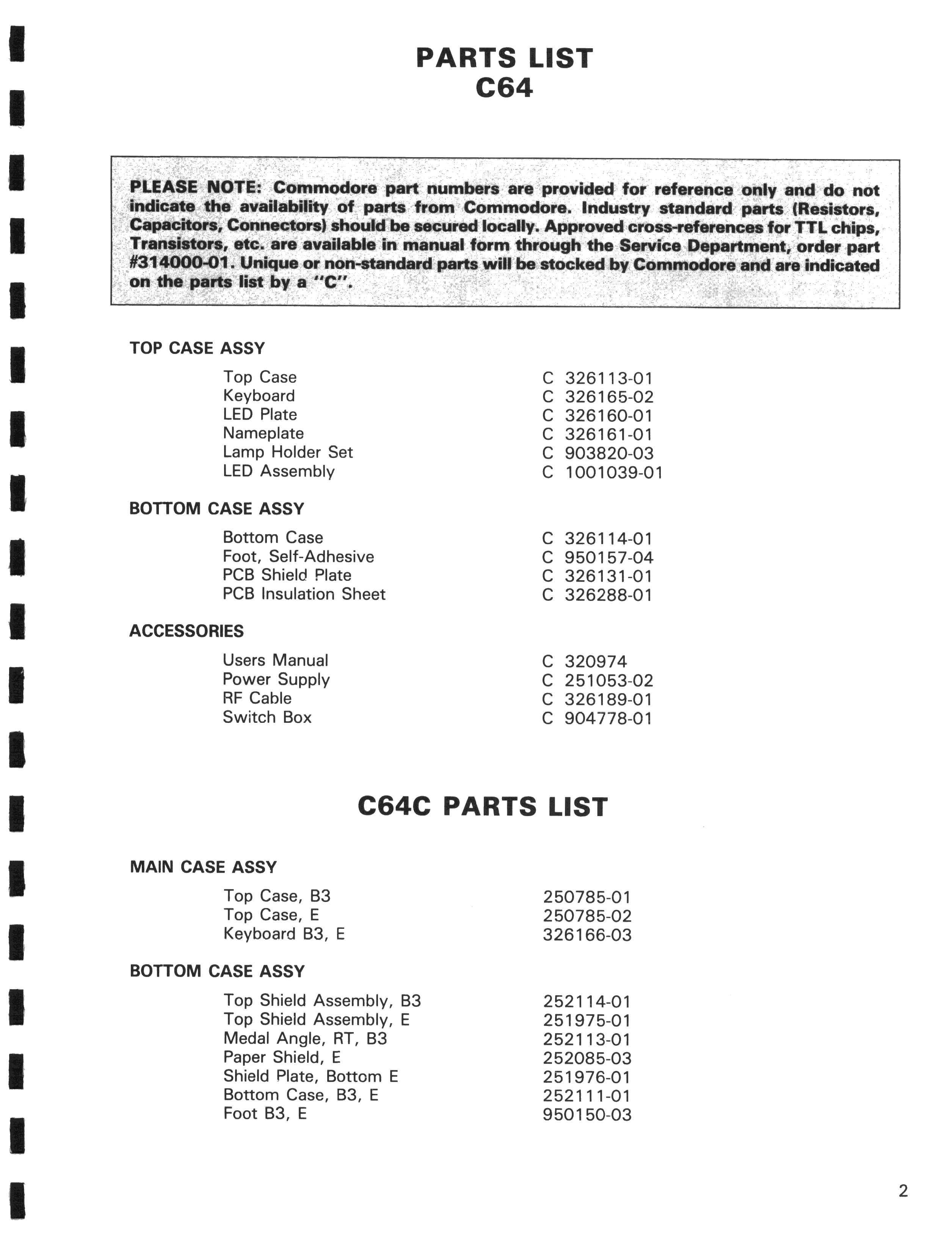
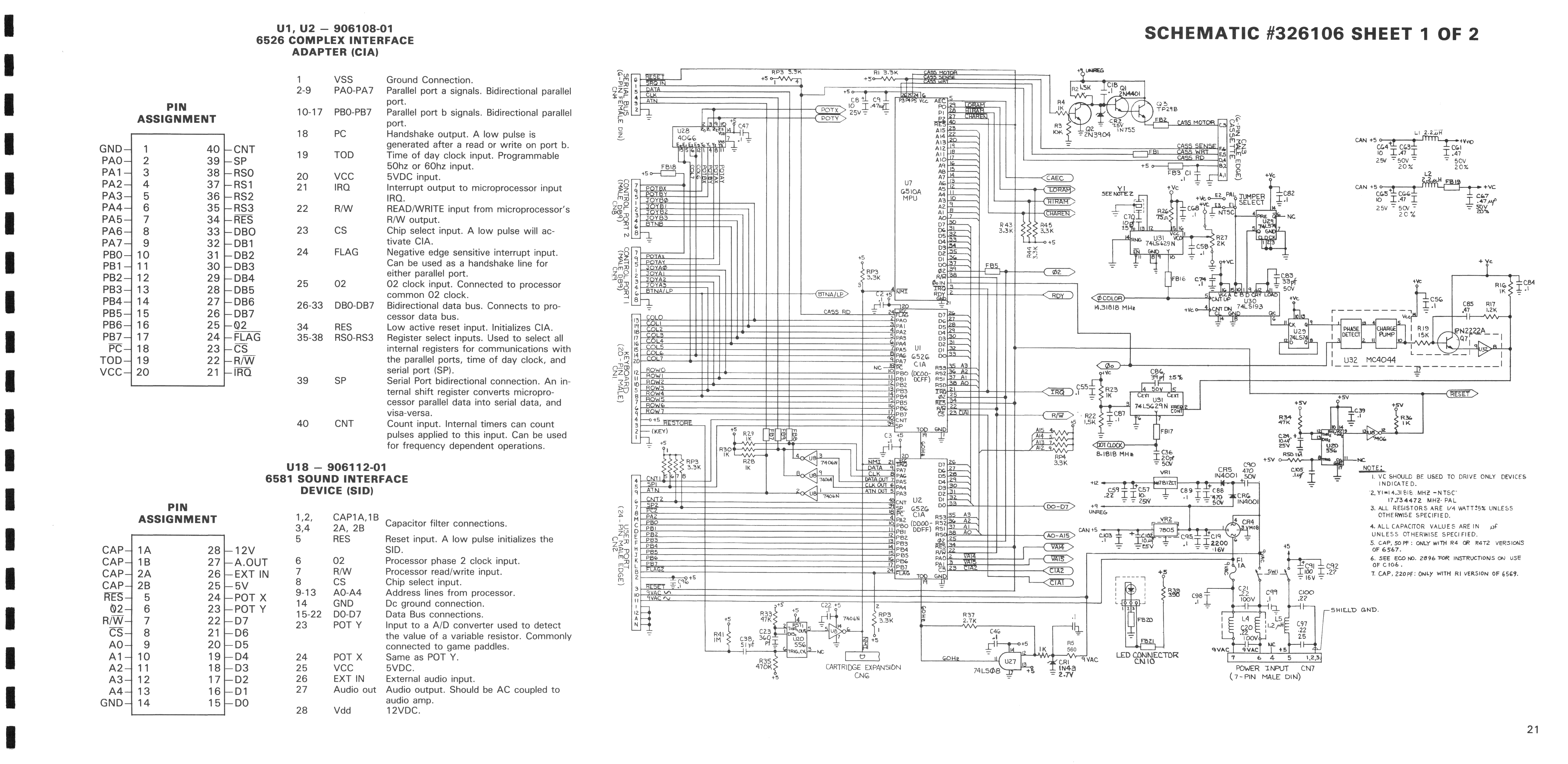
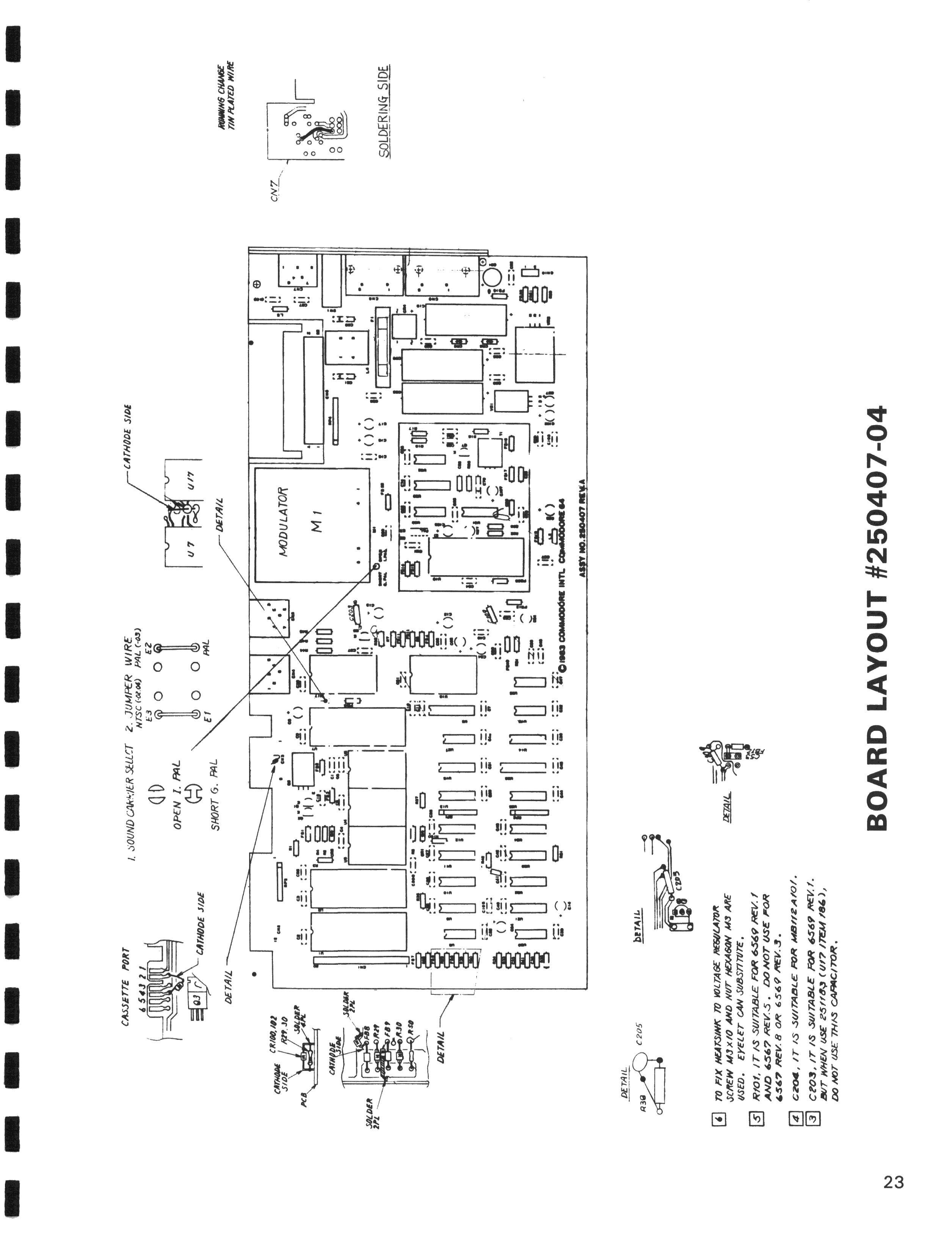
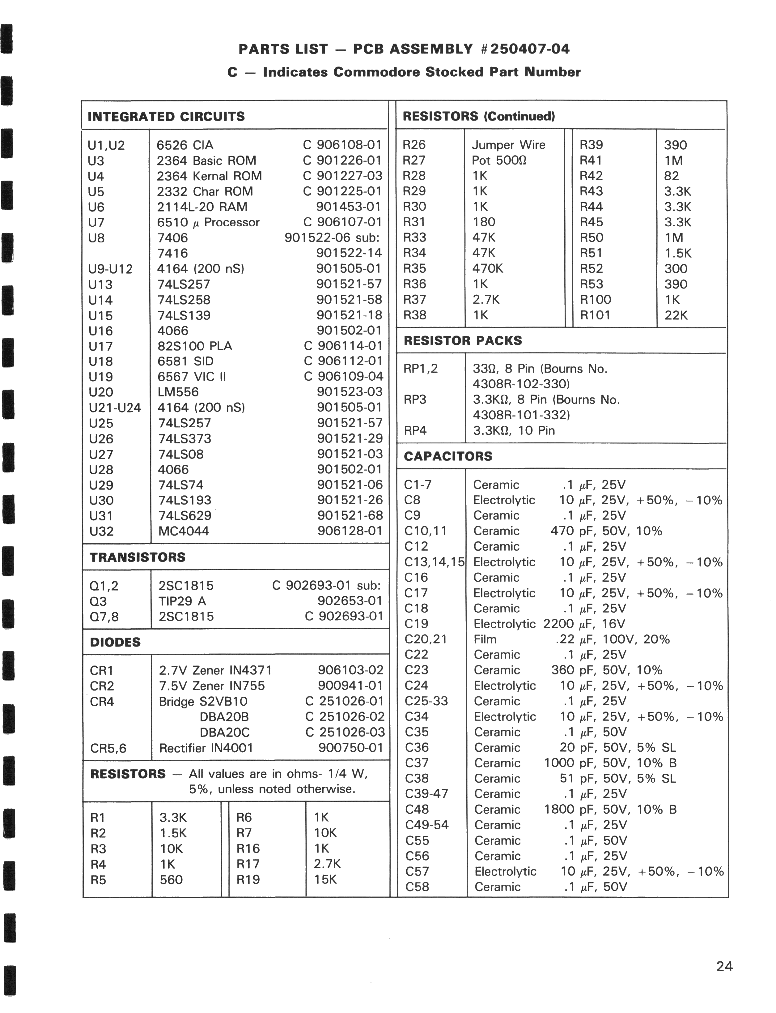
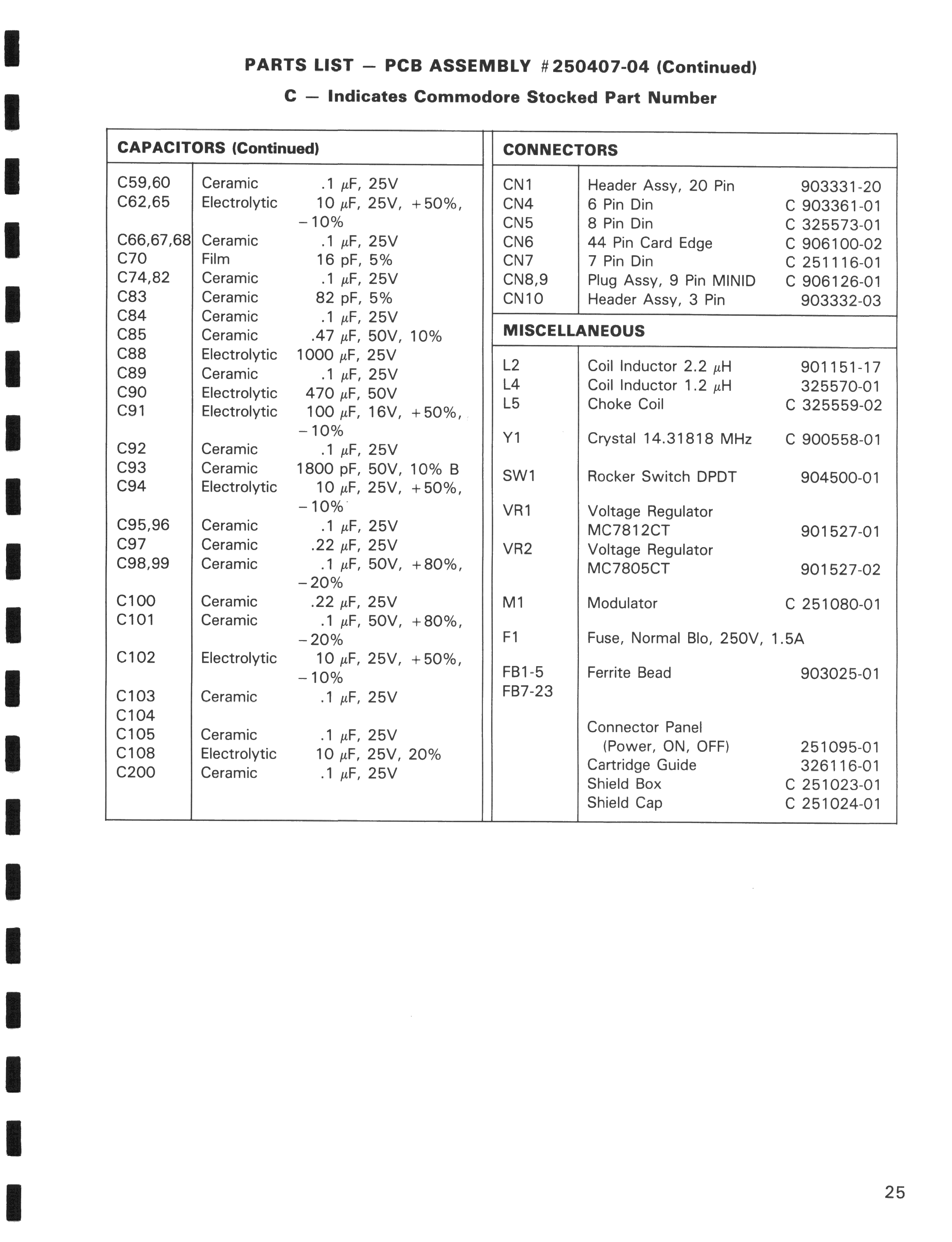
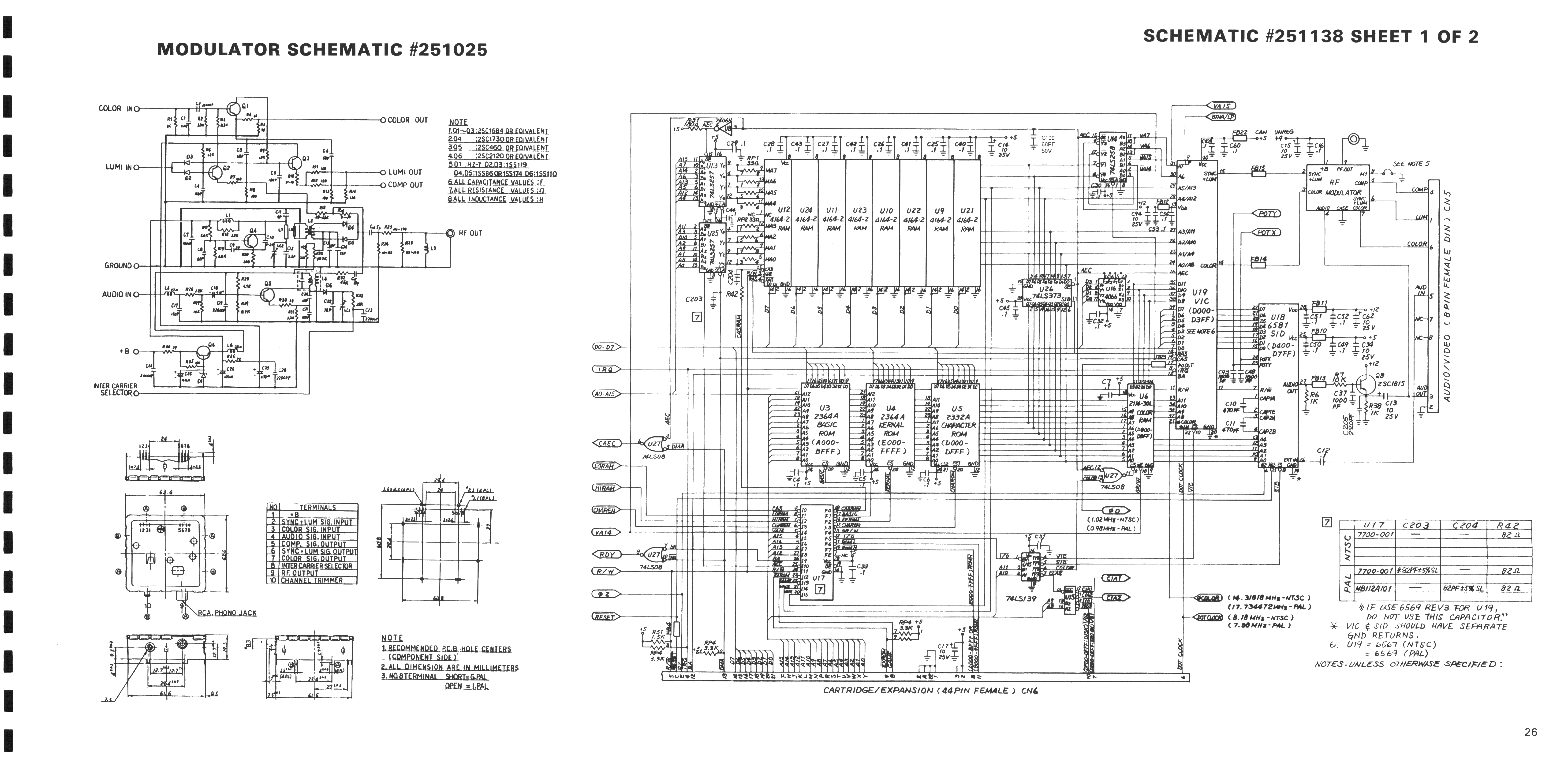
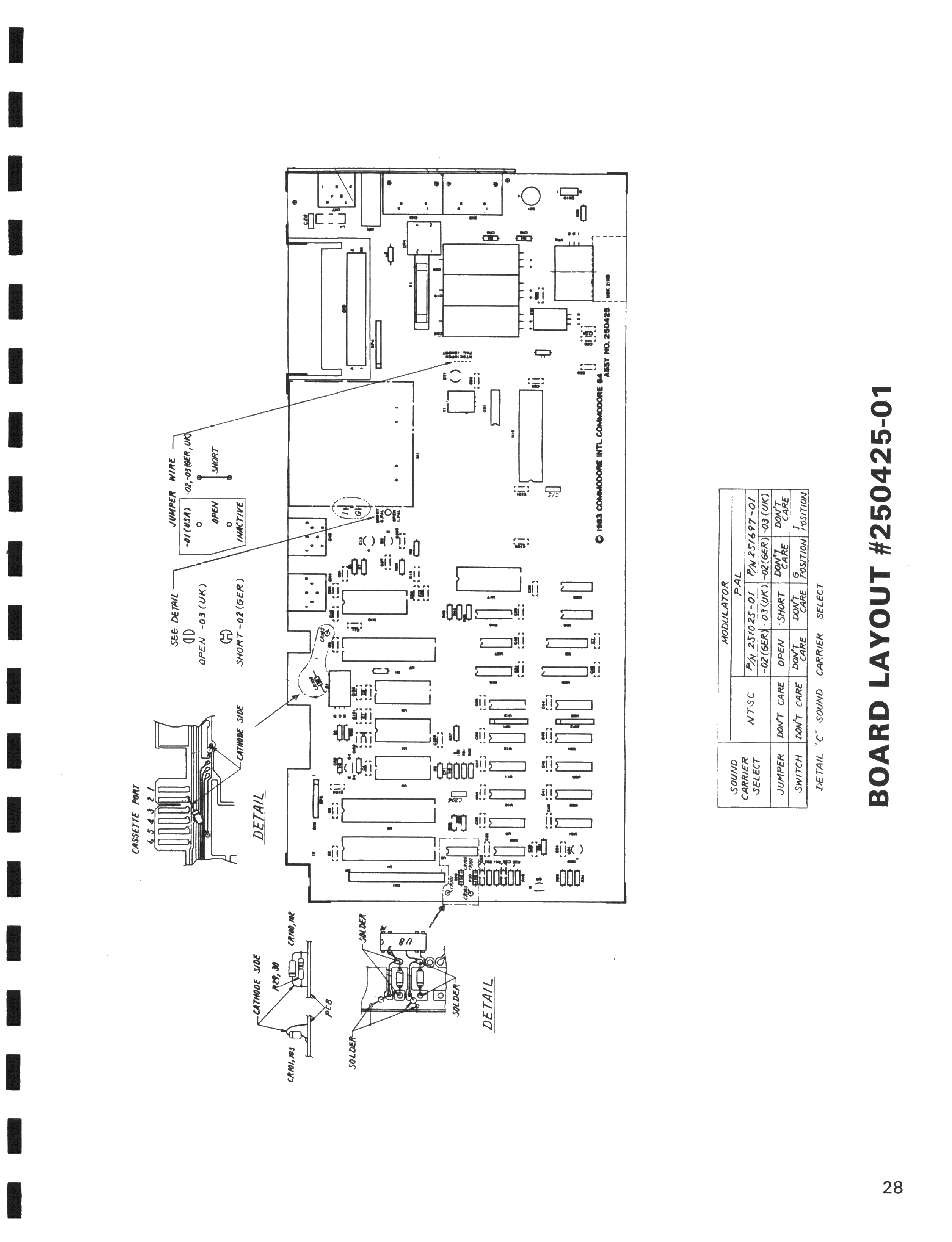
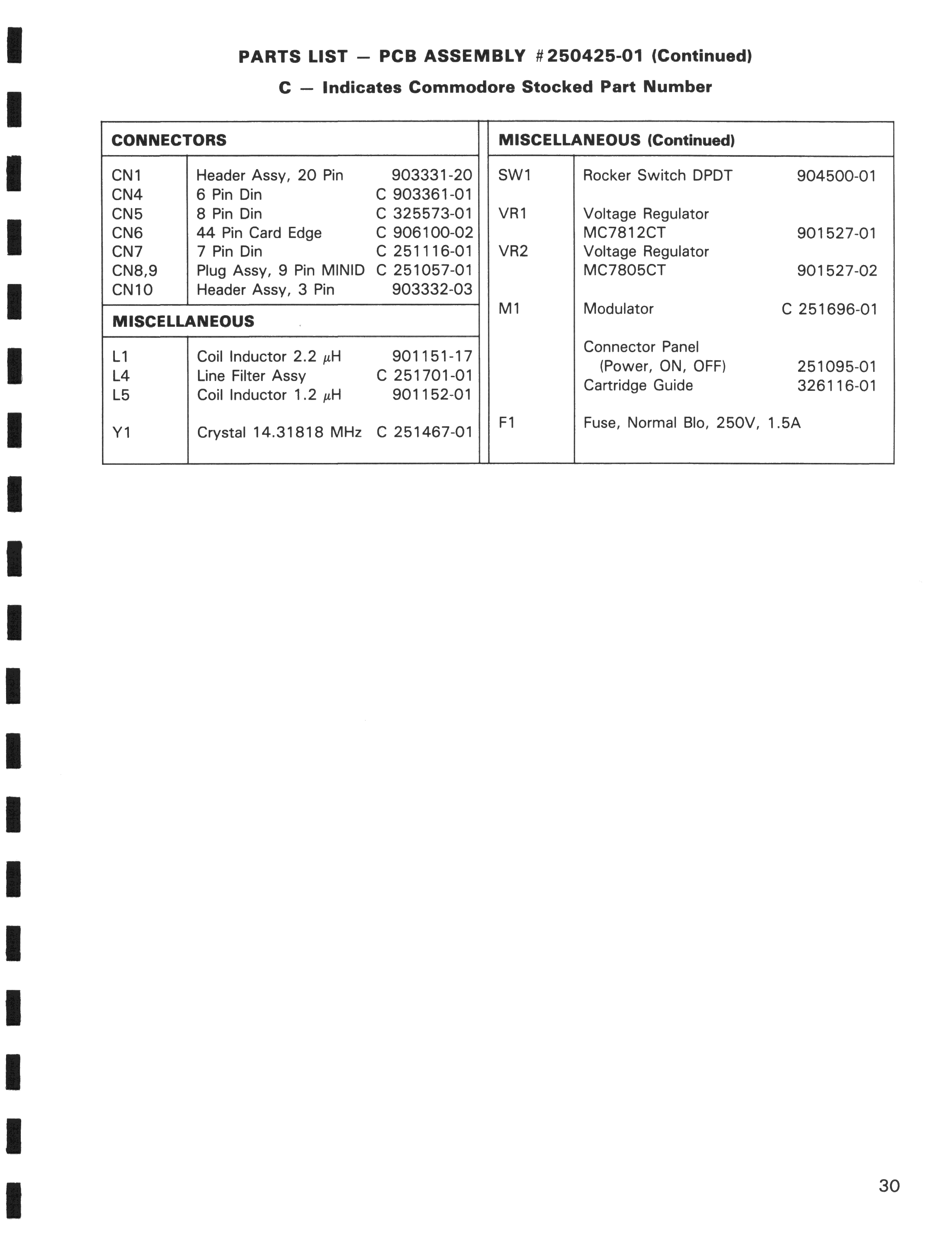
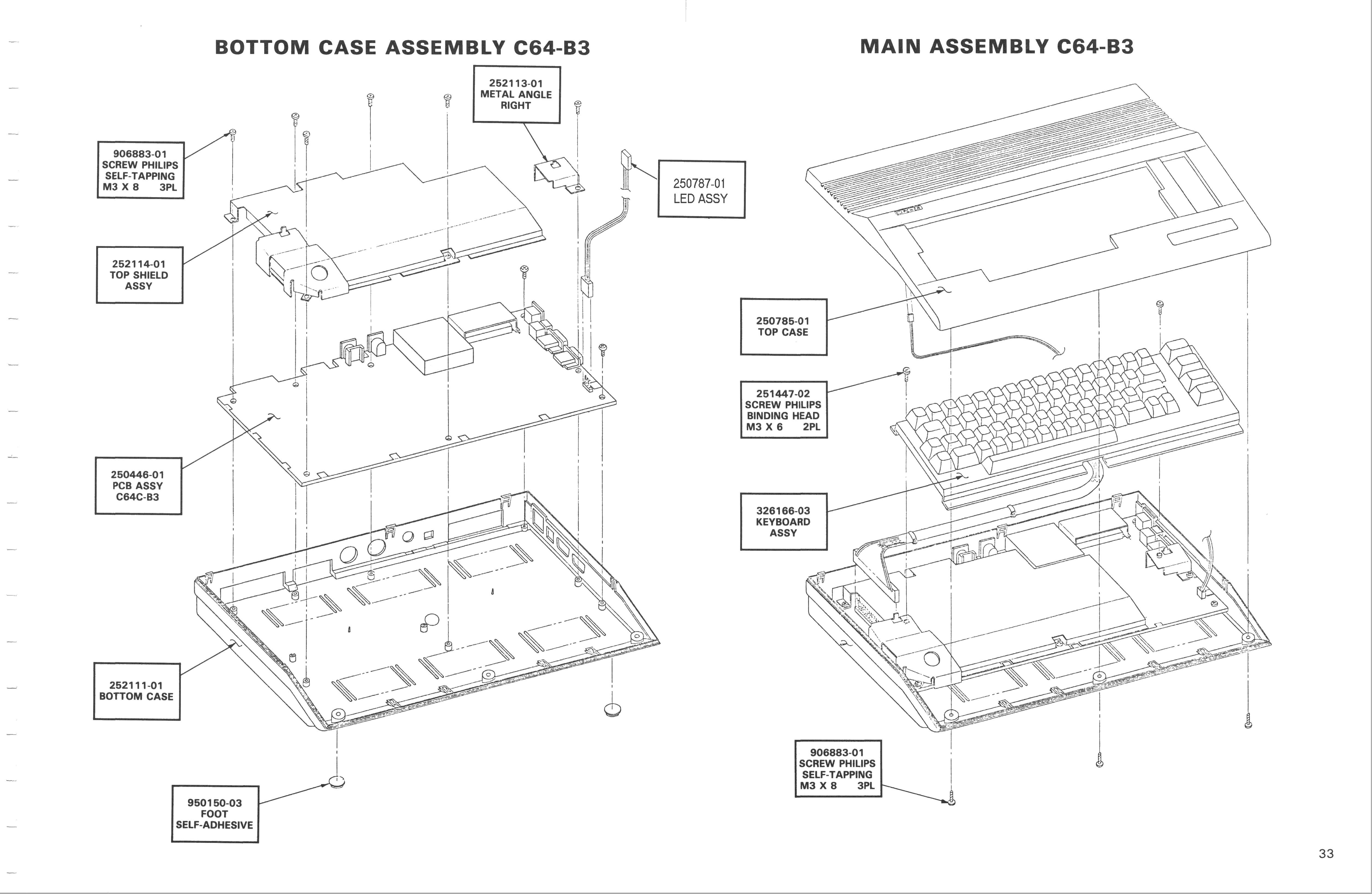
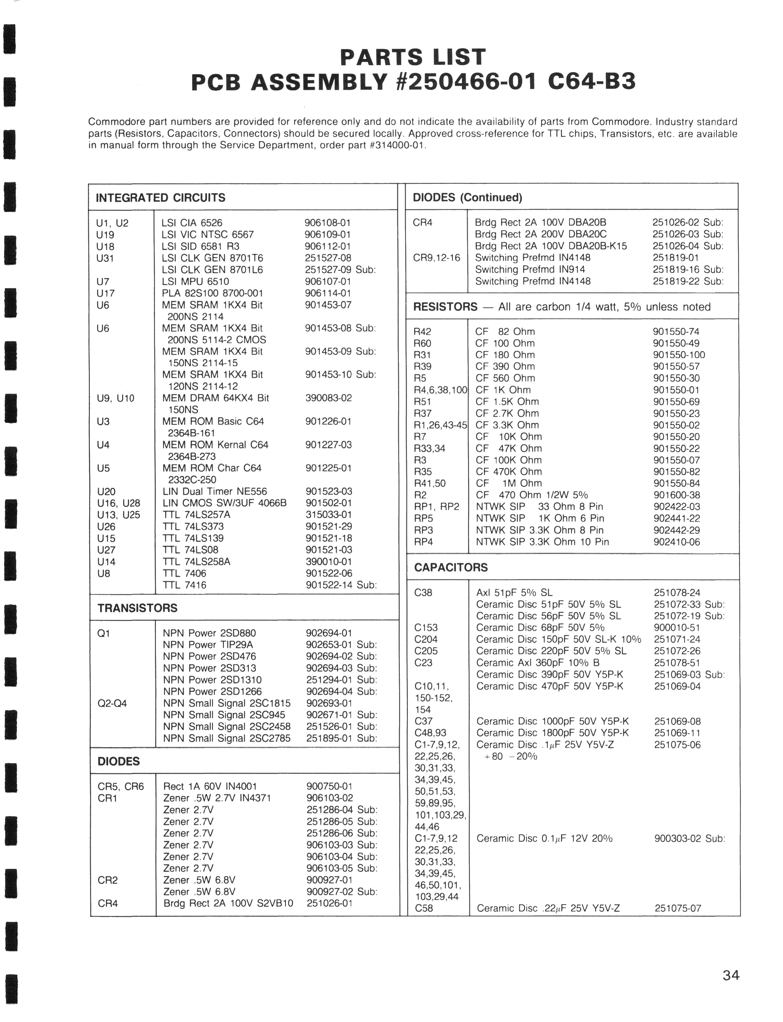
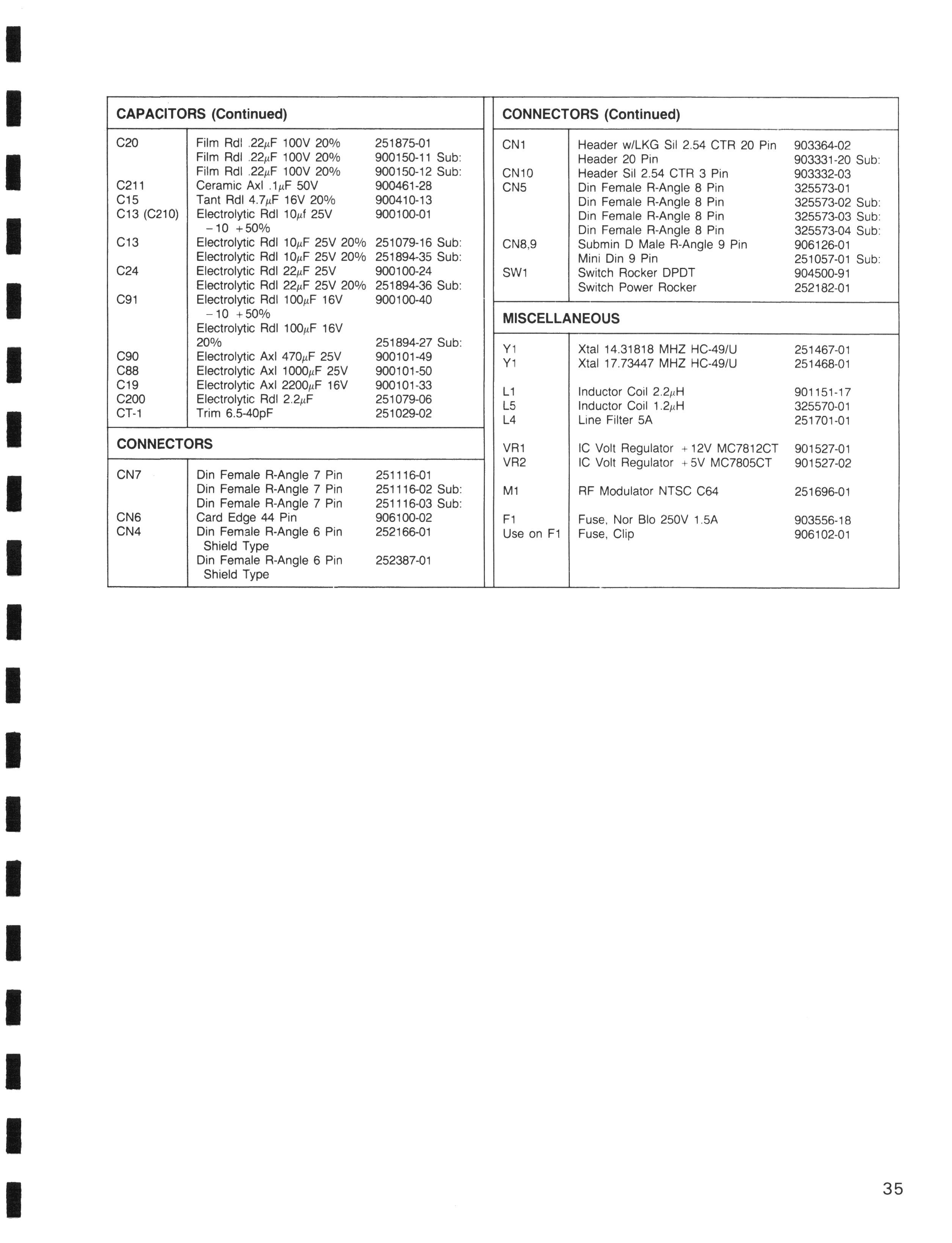
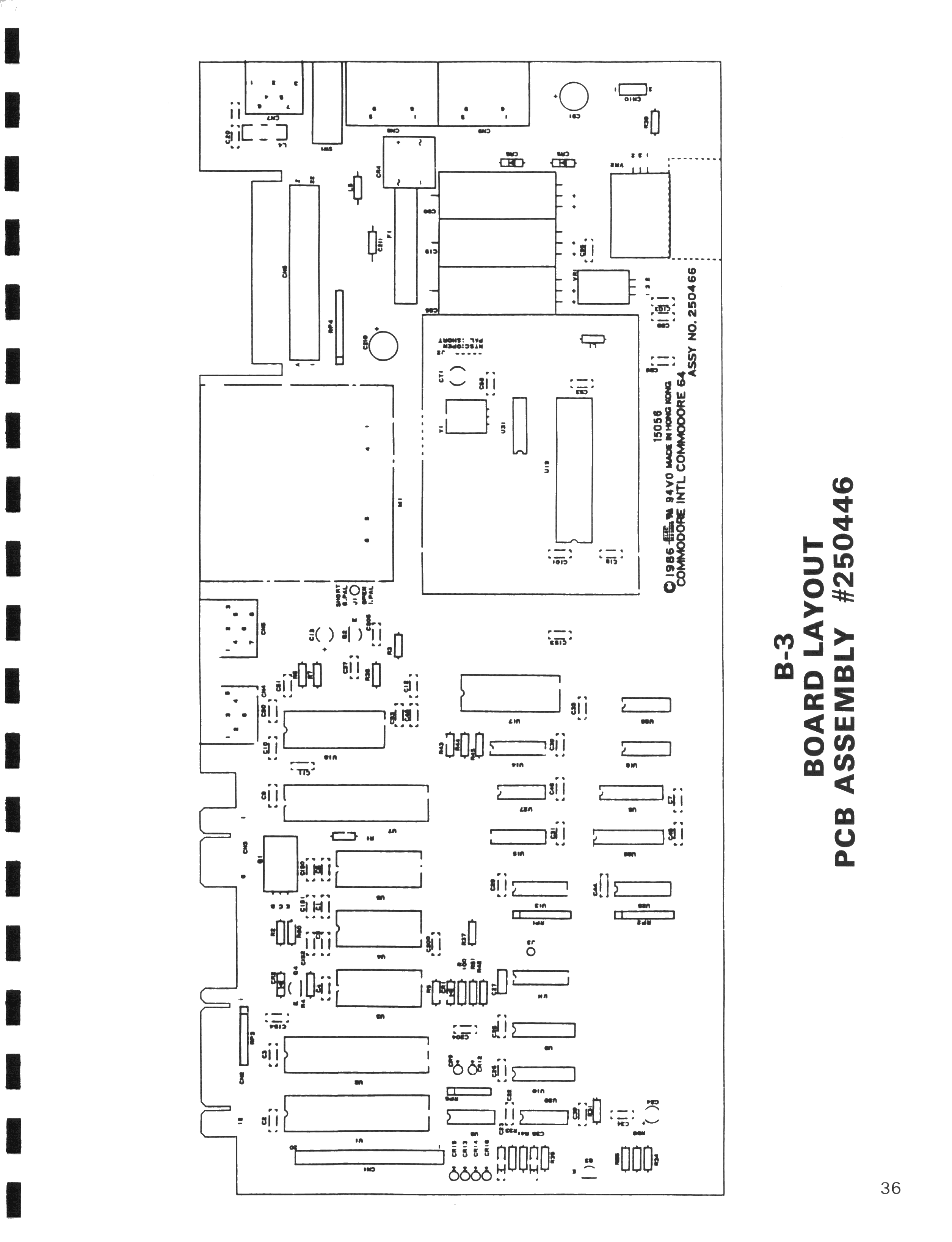
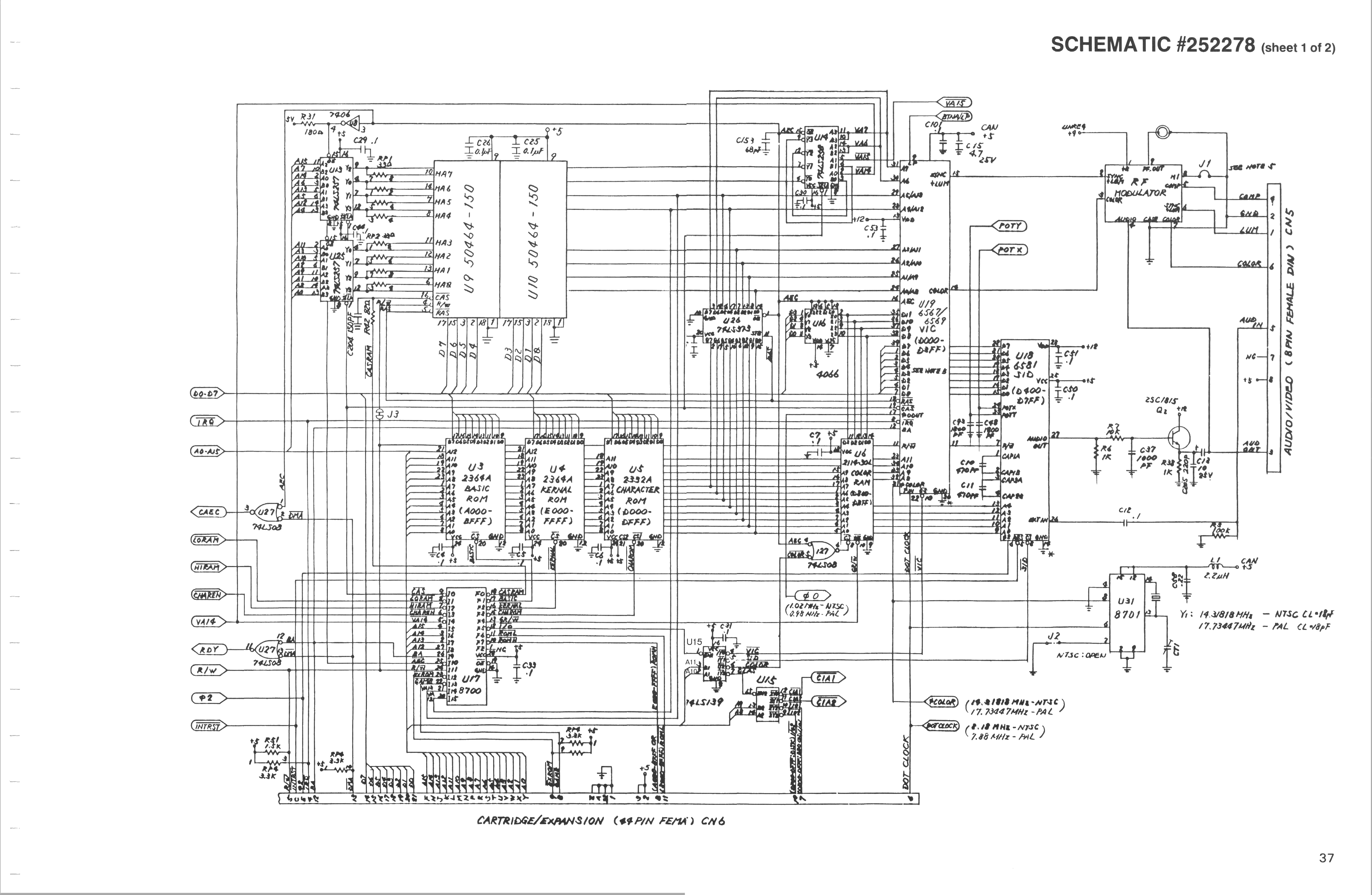
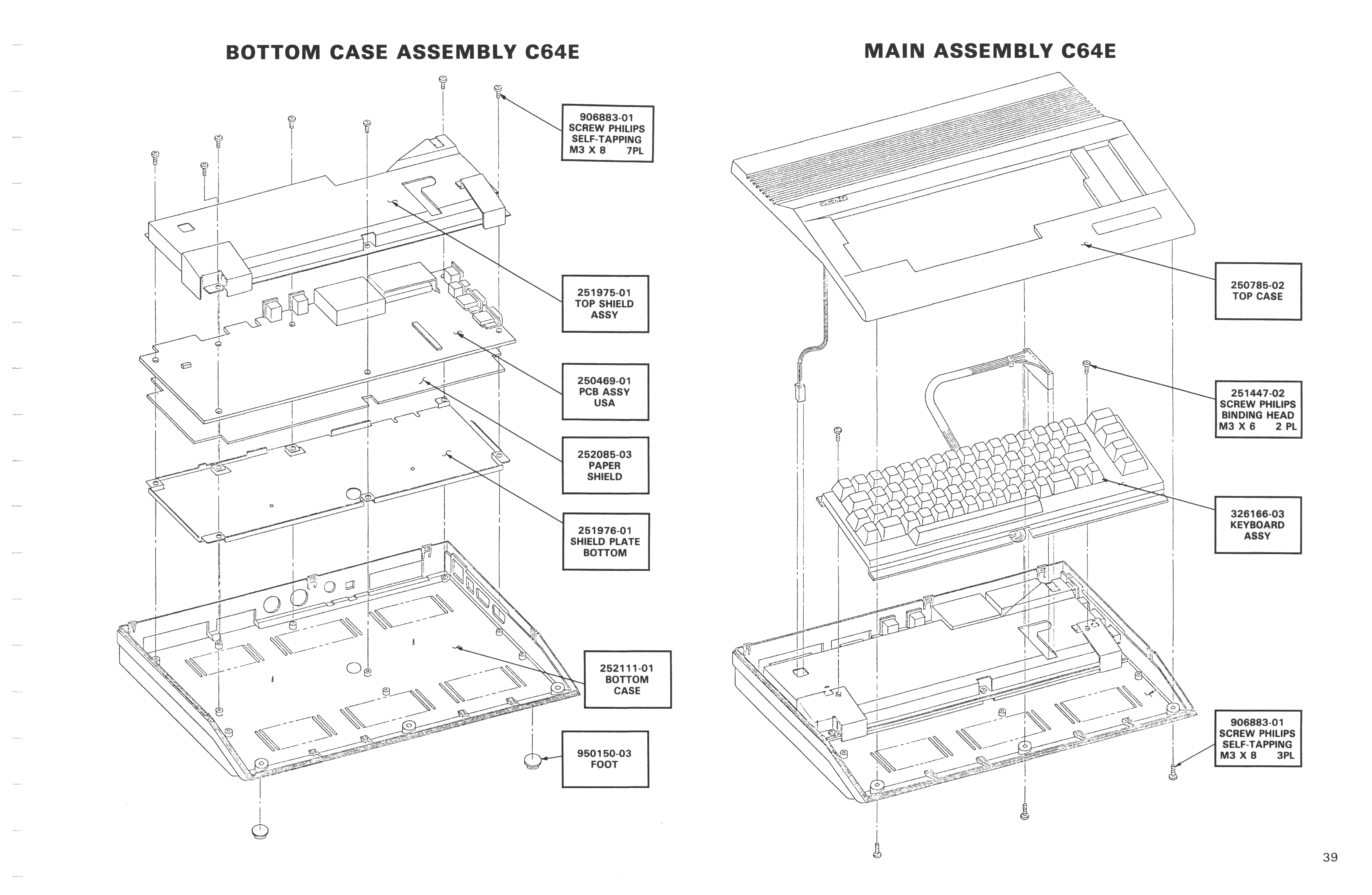
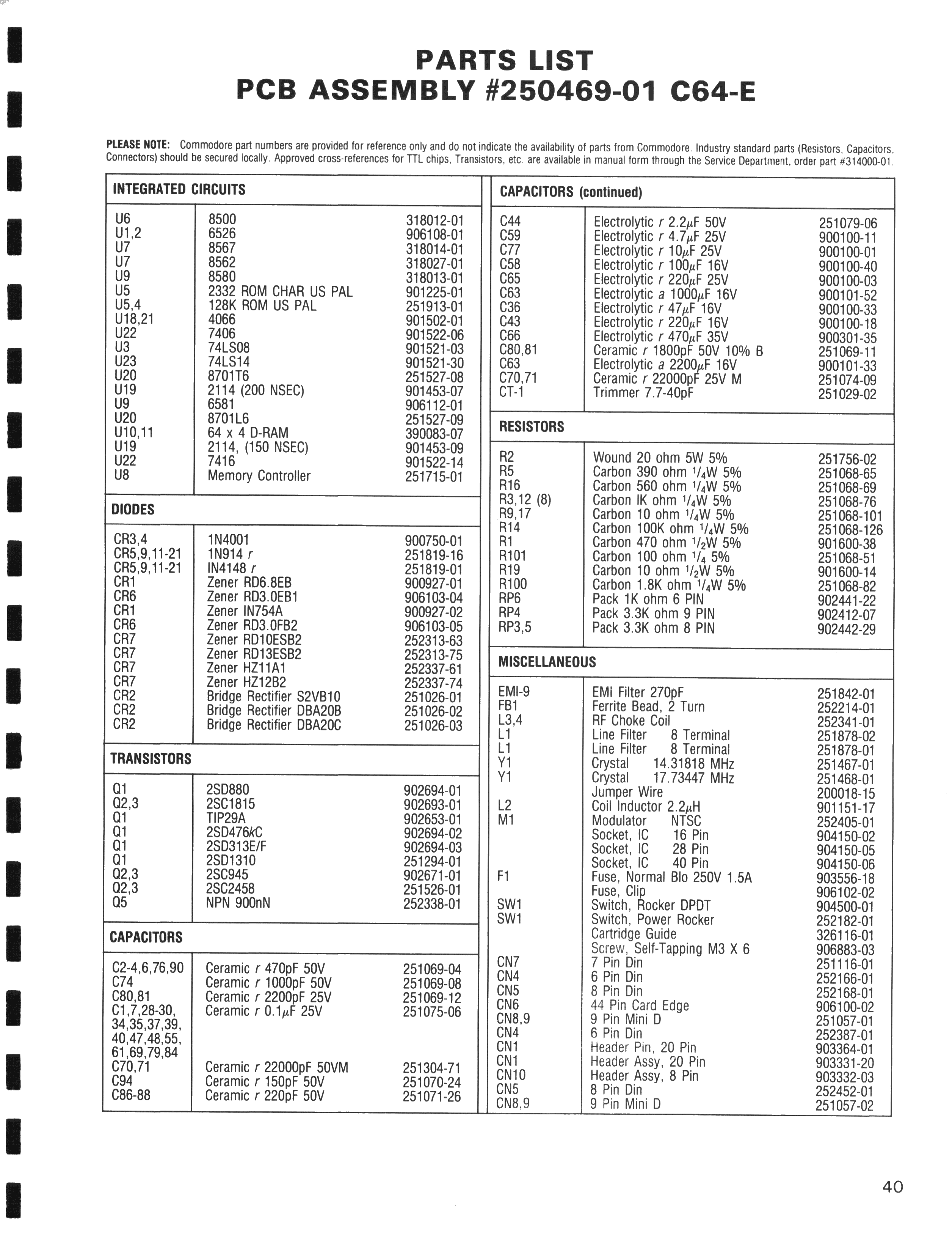
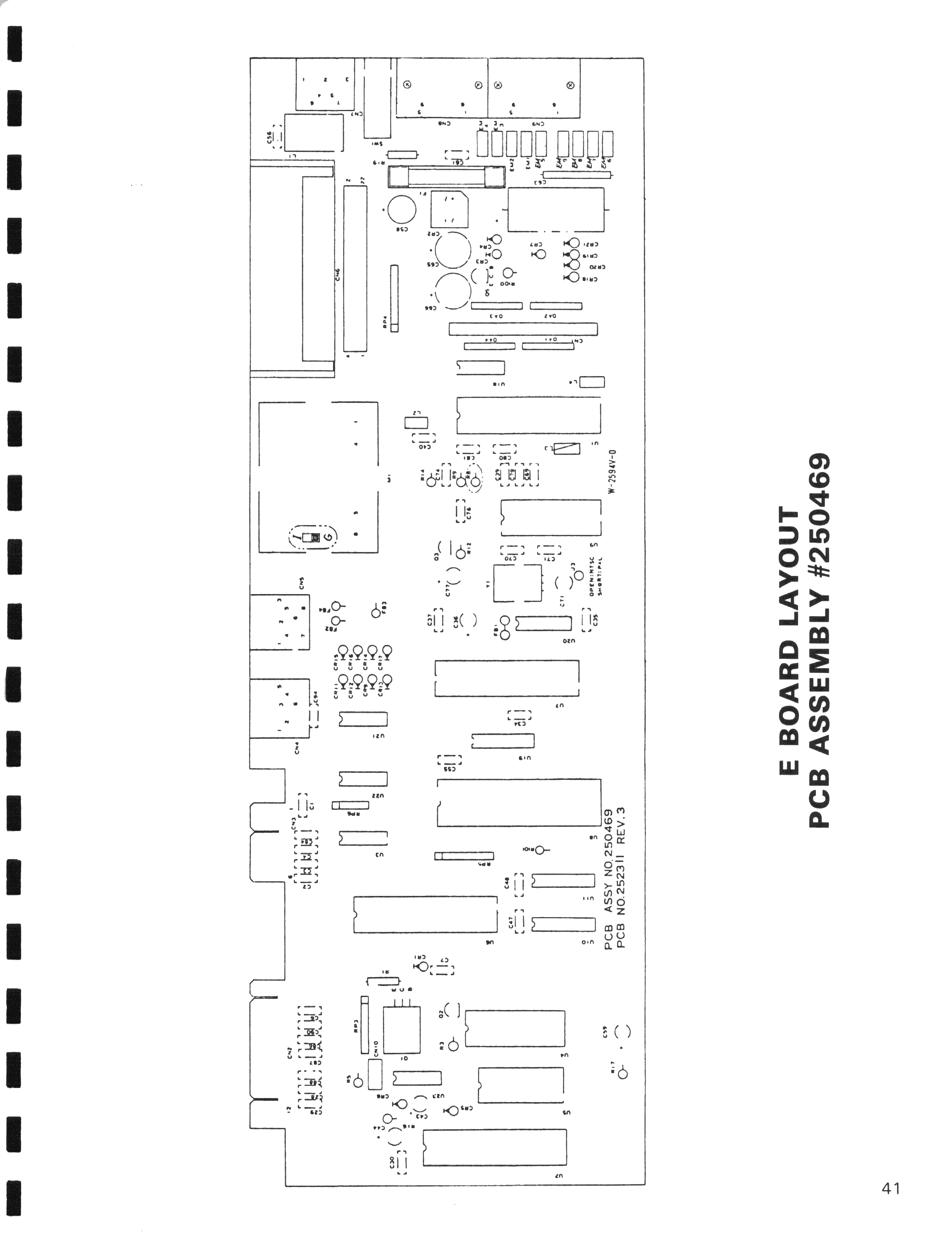
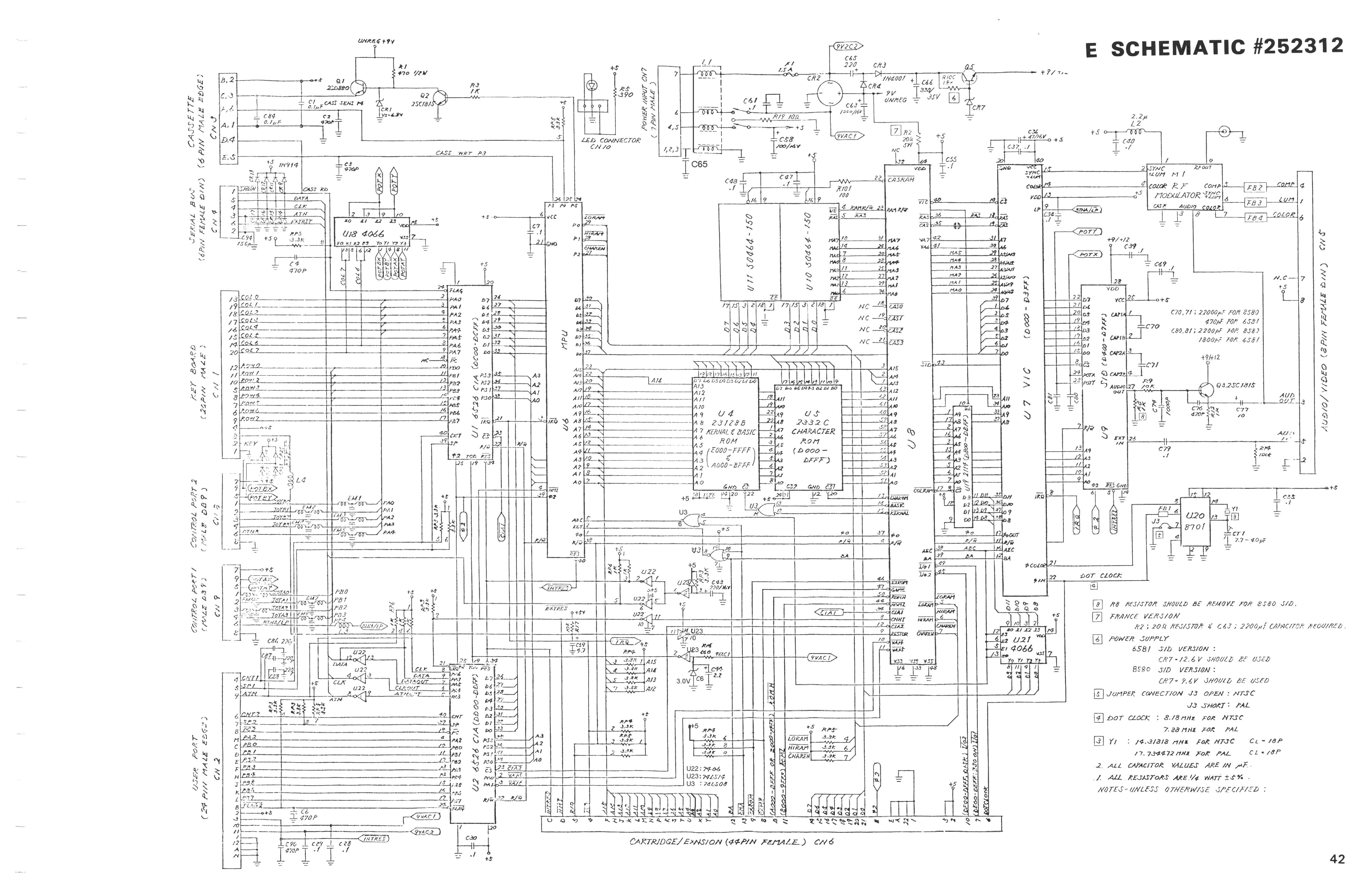
The scanned C64 Service Manual from 1992
- page:
title,
contents 1,
contents 2,
01,
02,
03,
04,
05,
06,
07,
08,
09,
10,
11,
12,
13,
14,
15,
16,
17,
18,
19,
20,
21,
22,
23,
24,
25,
26,
27,
28,
29,
30,
31,
32,
33,
34,
35,
36,
37,
38,
39,
40,
41,
42
Miscellaneous C64 schematics
- 250469-A-left,
250469-A-right,
250469-B-right:
Commodore 64c rev.A and rev.B (new design). The 64c boards have the
following texts: PCB ASSY NO. 250469 and PCB NO. 252311 REV.A (or B on
newer boards). The difference between the two revisions is in the Gate
Array chip: The one in rev.B includes COLOR RAM. That is why only the
right half of the schematic diagram differs. The REV.A schematics
also has the part number 252312.
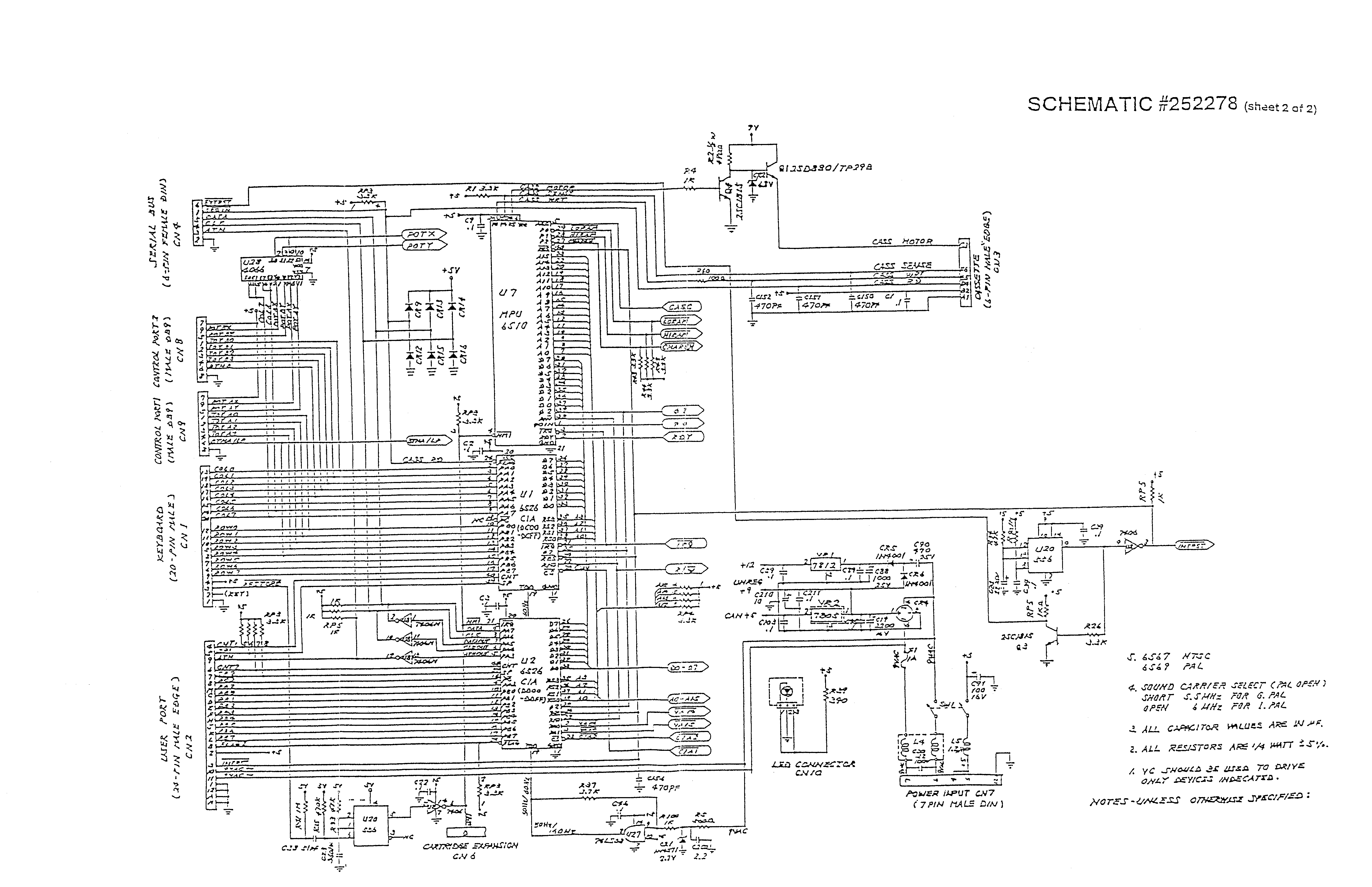
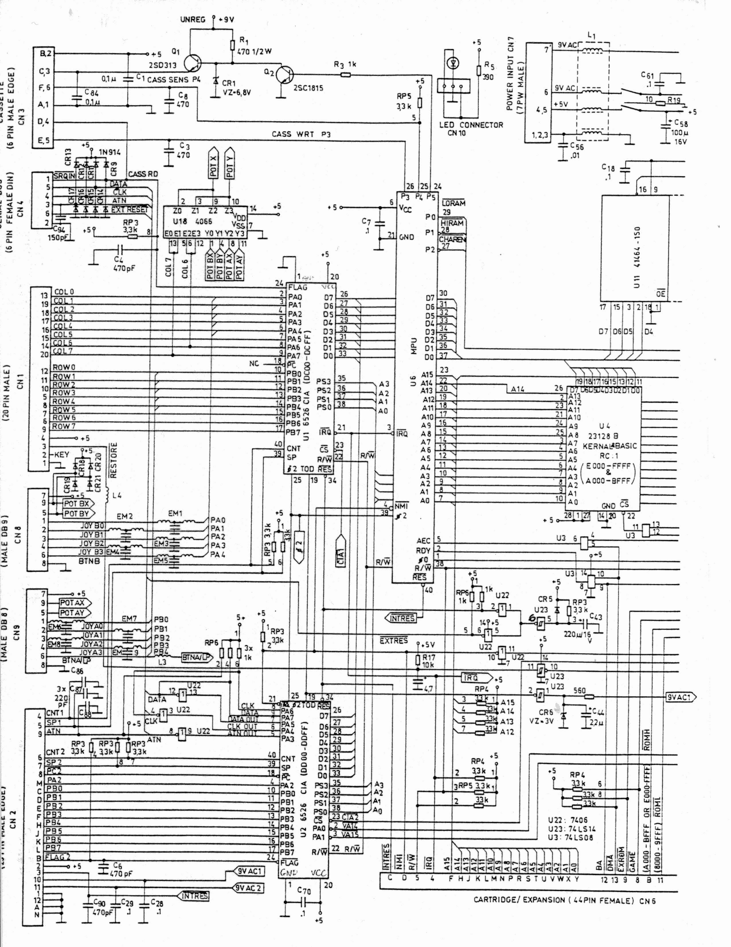
- 252278-1,
252278-2:
Commodore 64 schematic diagram 252278. This seems to be an intermediate
cost-reduced version, with 64kb x 4 memory chips but small ROMs.
- 252312-left,
252312-right:
A bit better scan of the 250469 REV.A, with 8 levels of gray.
- A block diagram of the Commodore 64 cassette I/O circuitry. Taken from the
SAMS C64 Troubleshooting Guide.
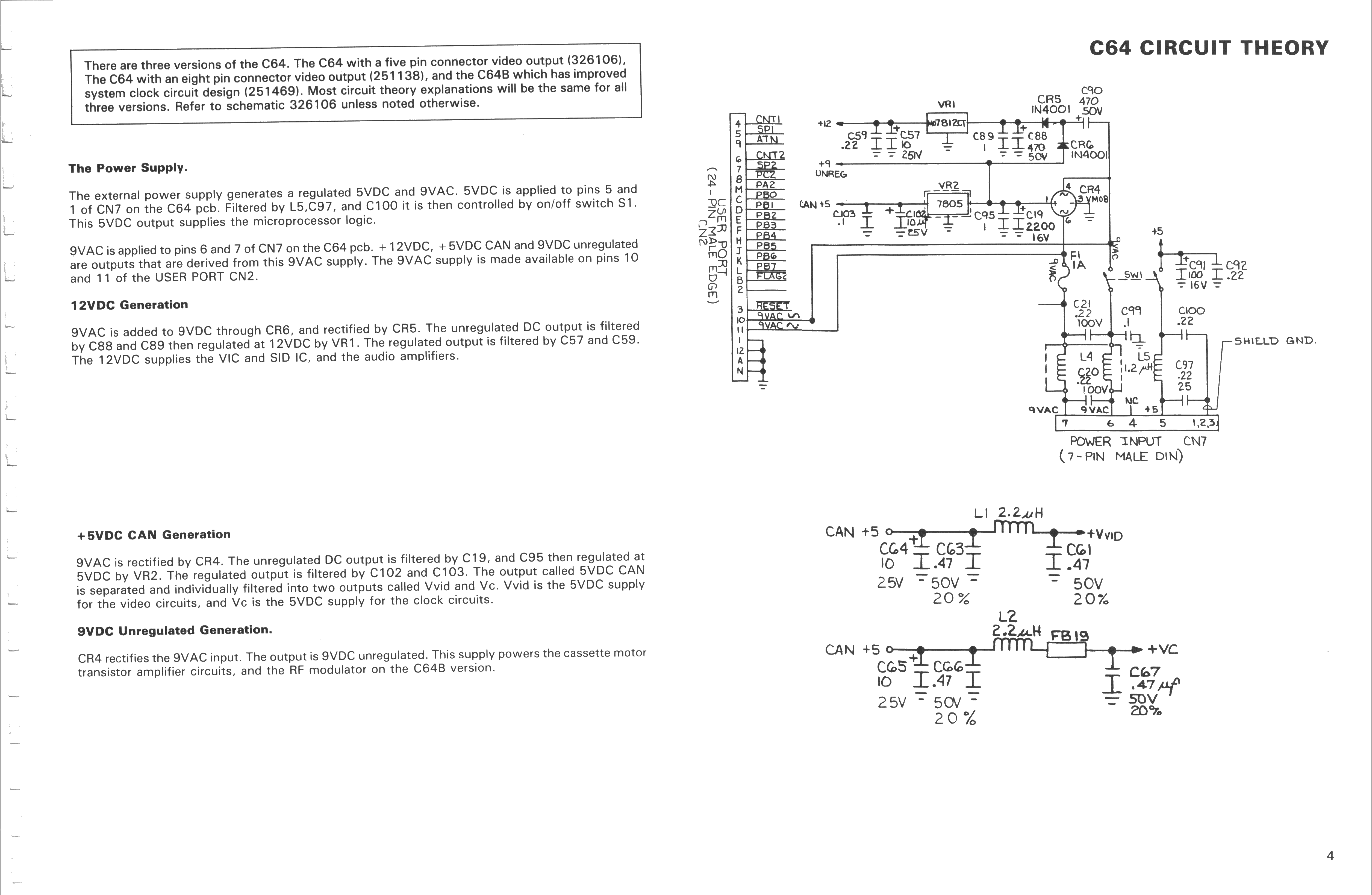
- A block diagram of the Commodore 64 internal power supply (how the
+12V, +9V and TOD clock signals are generated from the 9V AC input).
Taken from the SAMS C64 Troubleshooting Guide.
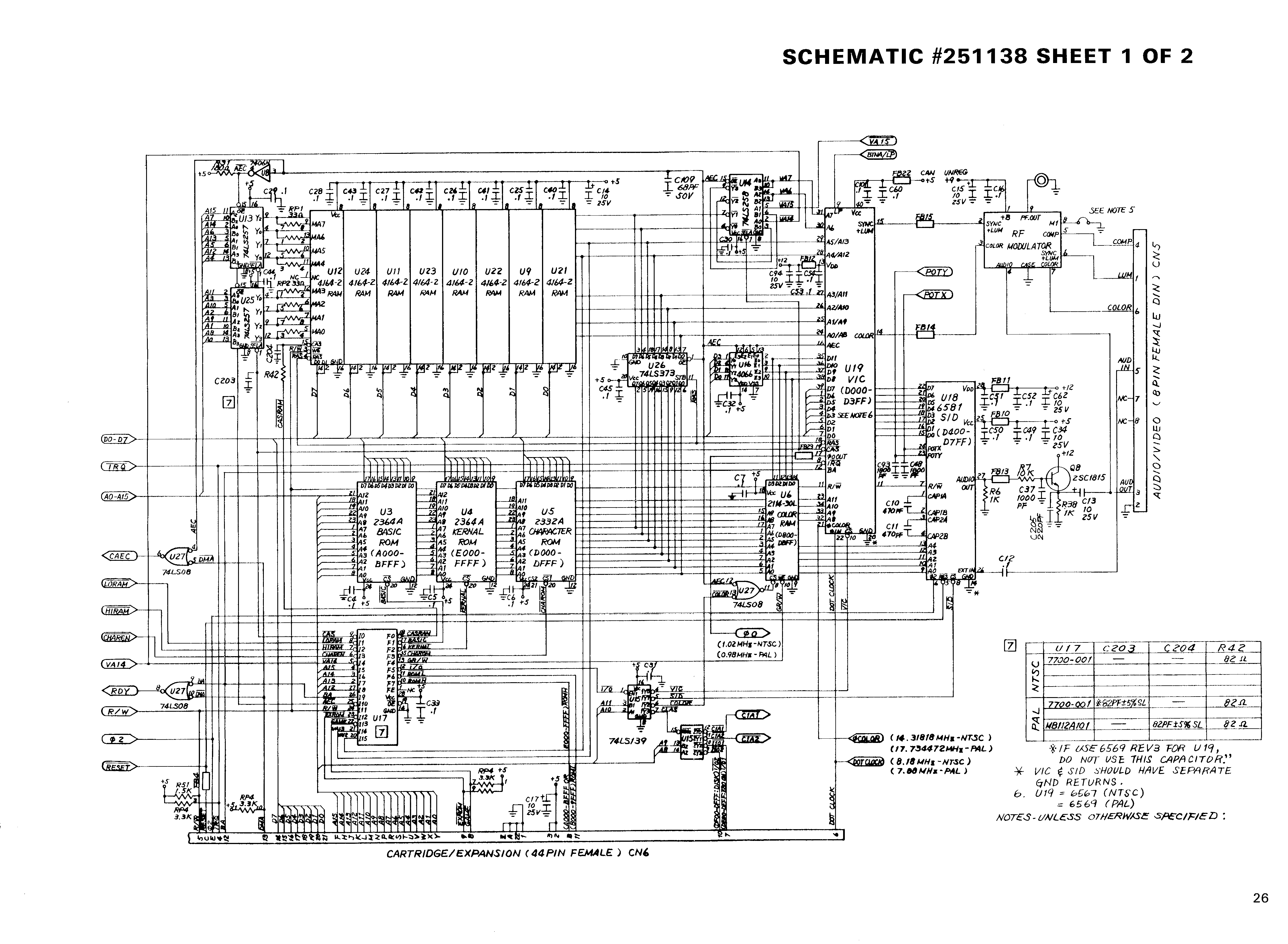
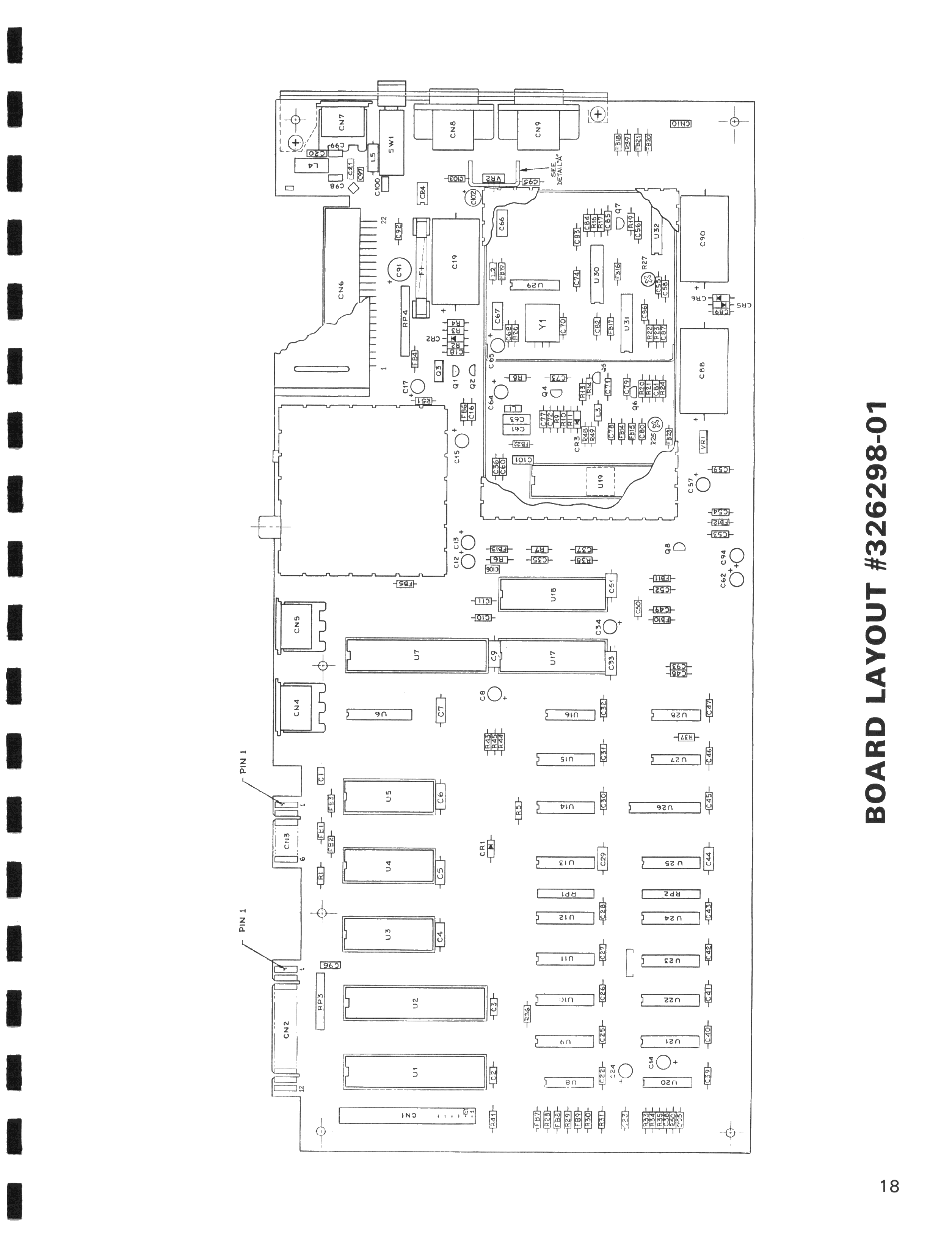
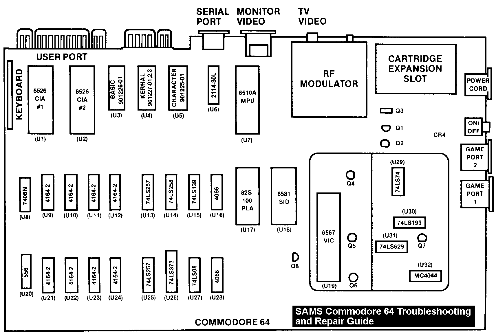
- A chip location diagram of the first C64 board revision. Assy number
unknown, or maybe 251138. Taken from the SAMS C64 Troubleshooting Guide.
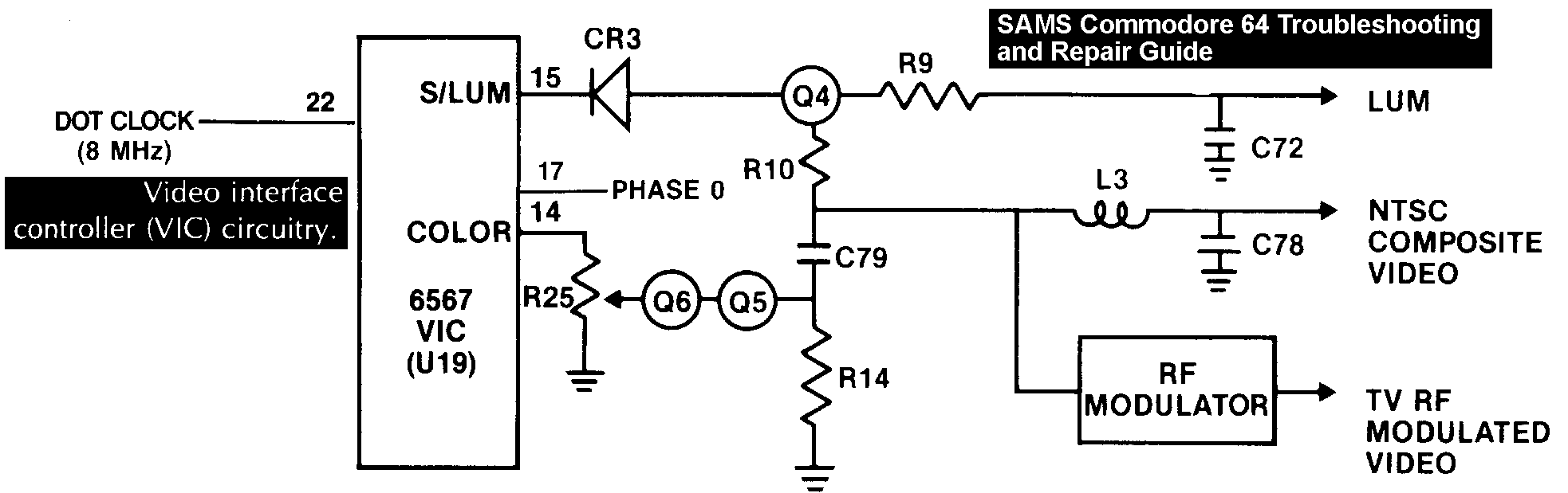
- A block diagram of the video circuitry in the first C64 board revision.
Taken from the SAMS C64 Troubleshooting Guide.
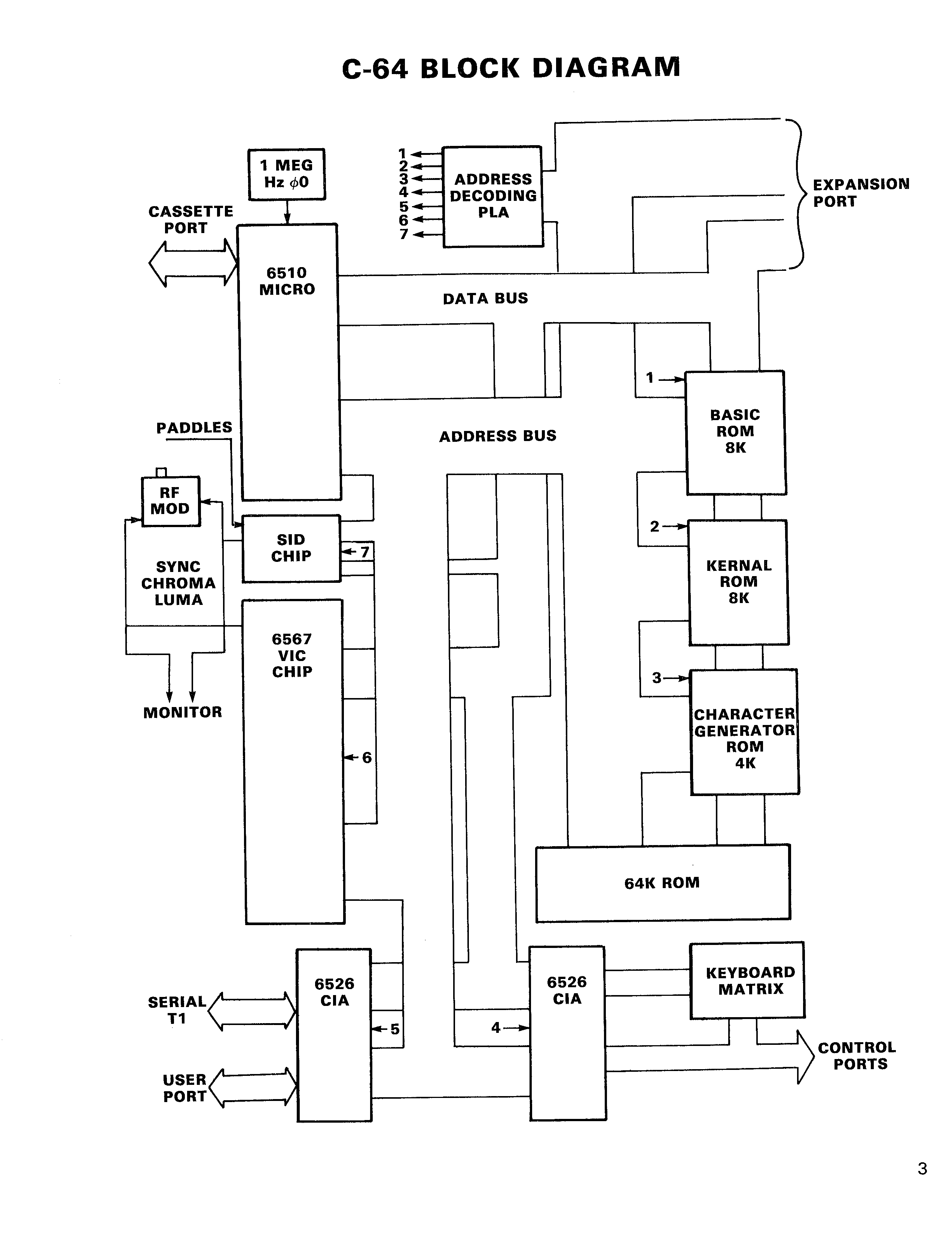
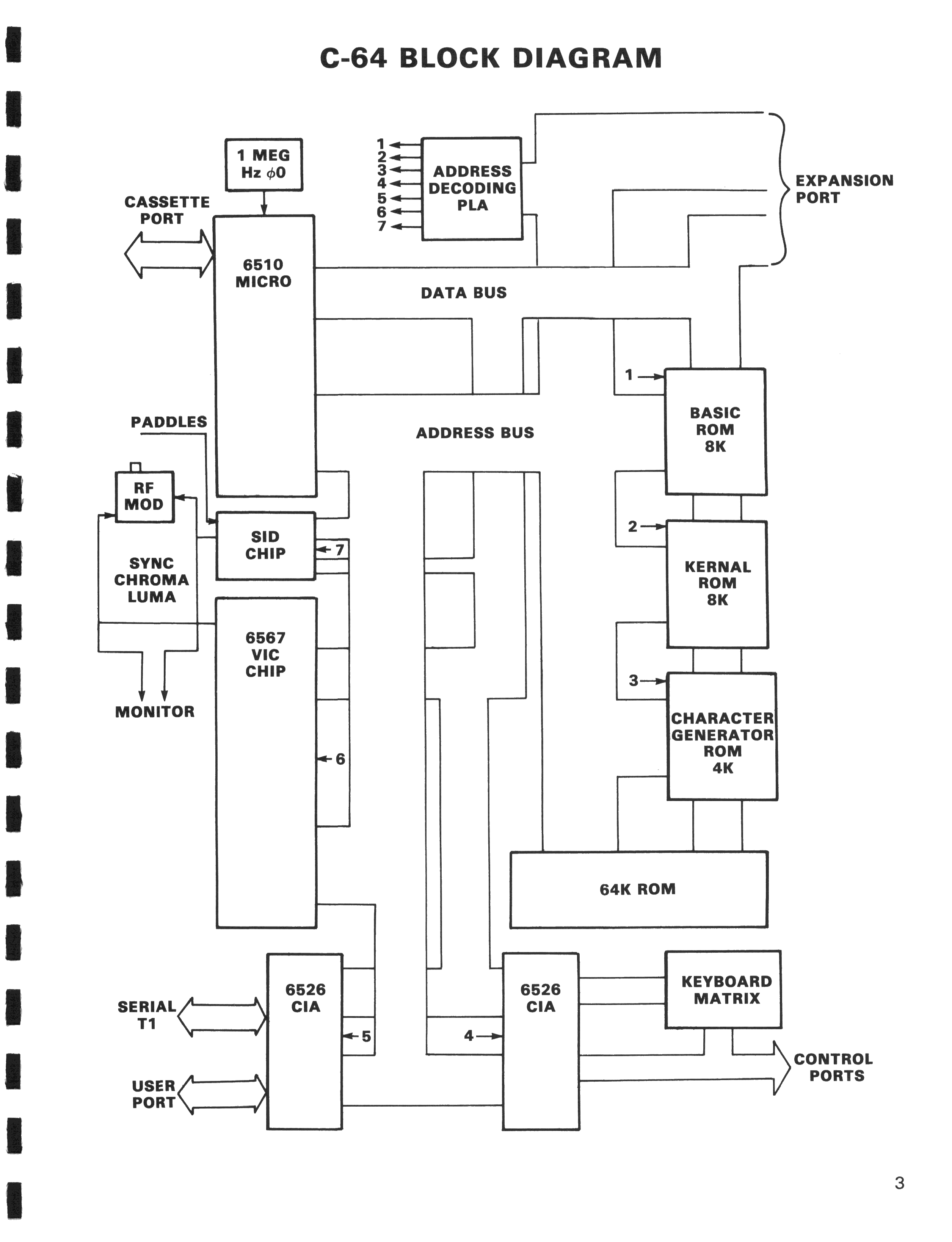
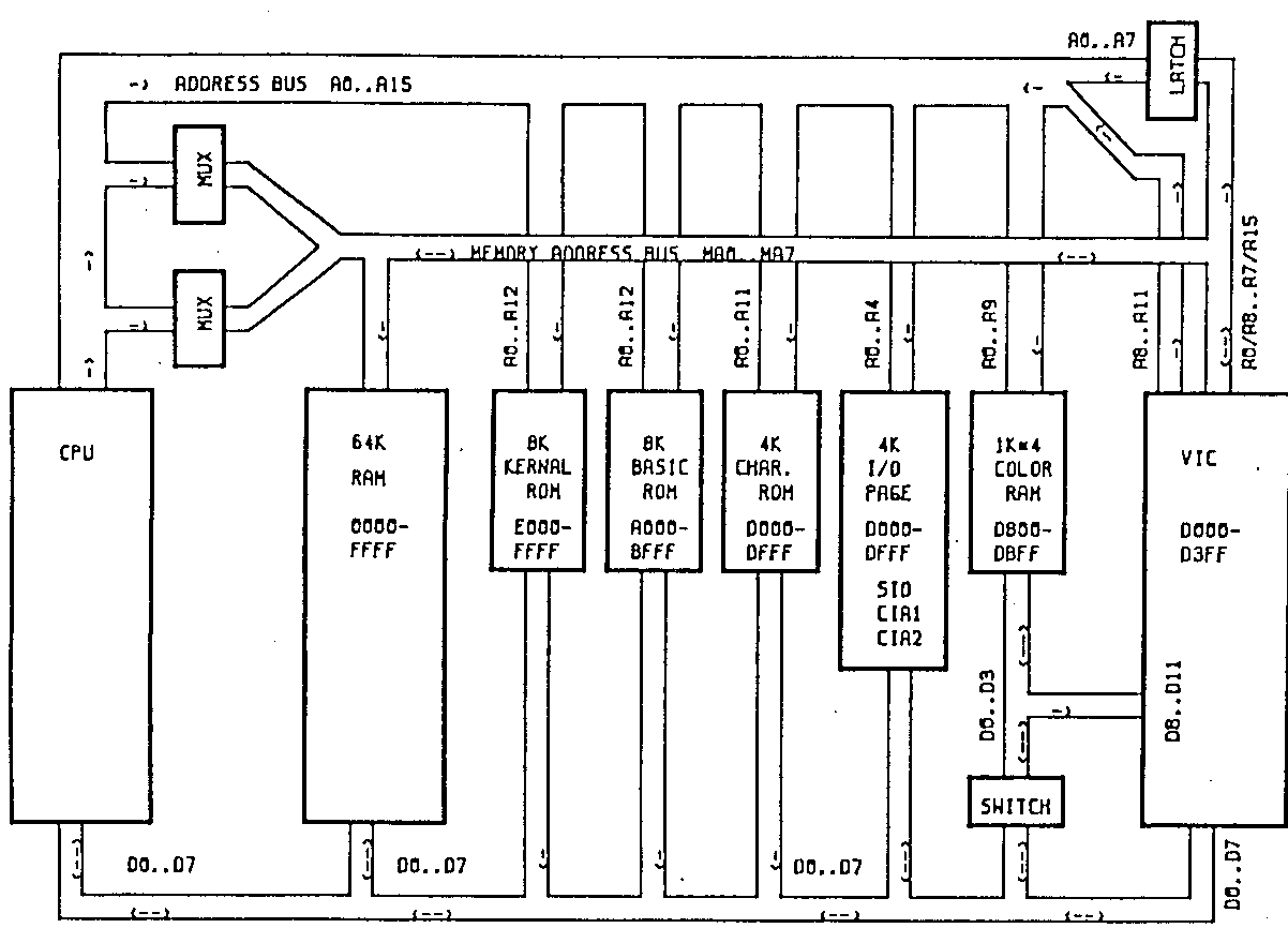
- A block diagram of the bus signals in the C64.
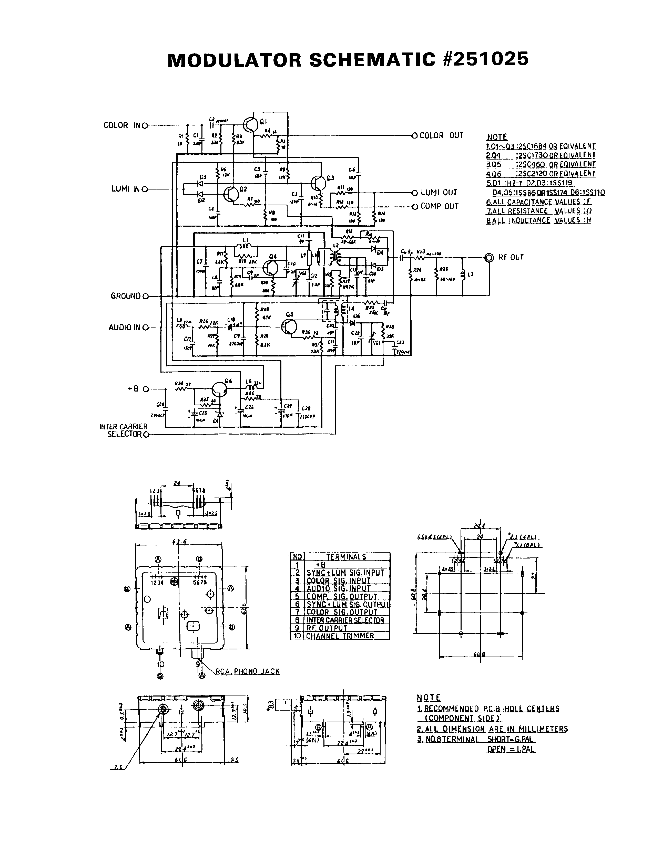
- Commodore 64 Power Supply, part no. 902503-02, input 116V 60Hz 40W.
This is the North American power supply that can be taken apart.
The schematic was drawn by William Levak. According to him, the
transistor and the 300 ohm resistor can be removed and replaced with a
standard +5V 750mA voltage regulator, which is much more reliable.
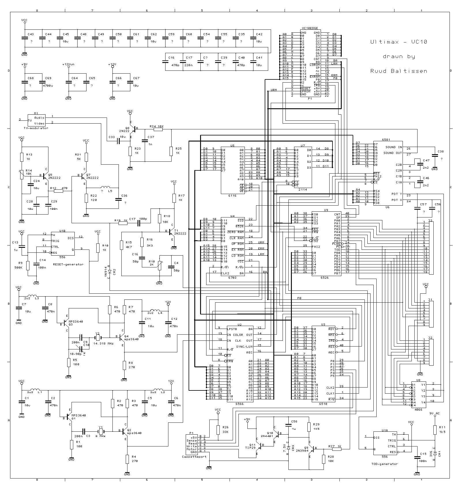
- Commodore VIC-10, a.k.a. UltiMax a.k.a. "Vickie" schematic diagram, drawn
by Ruud Baltissen. For more information on this extremely rare machine,
see www.hut.fi/Misc/cbm/docs/ultimax.html.
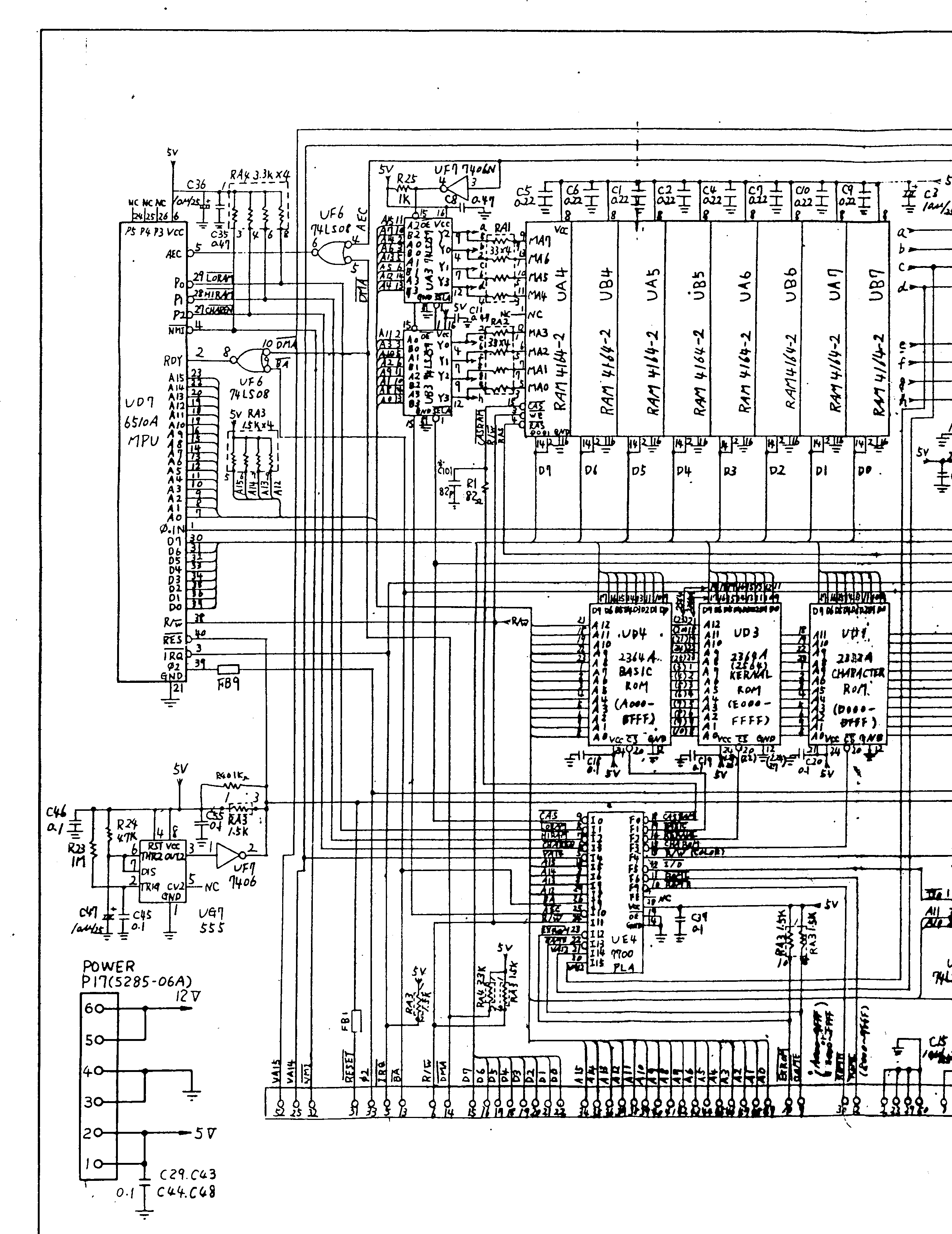
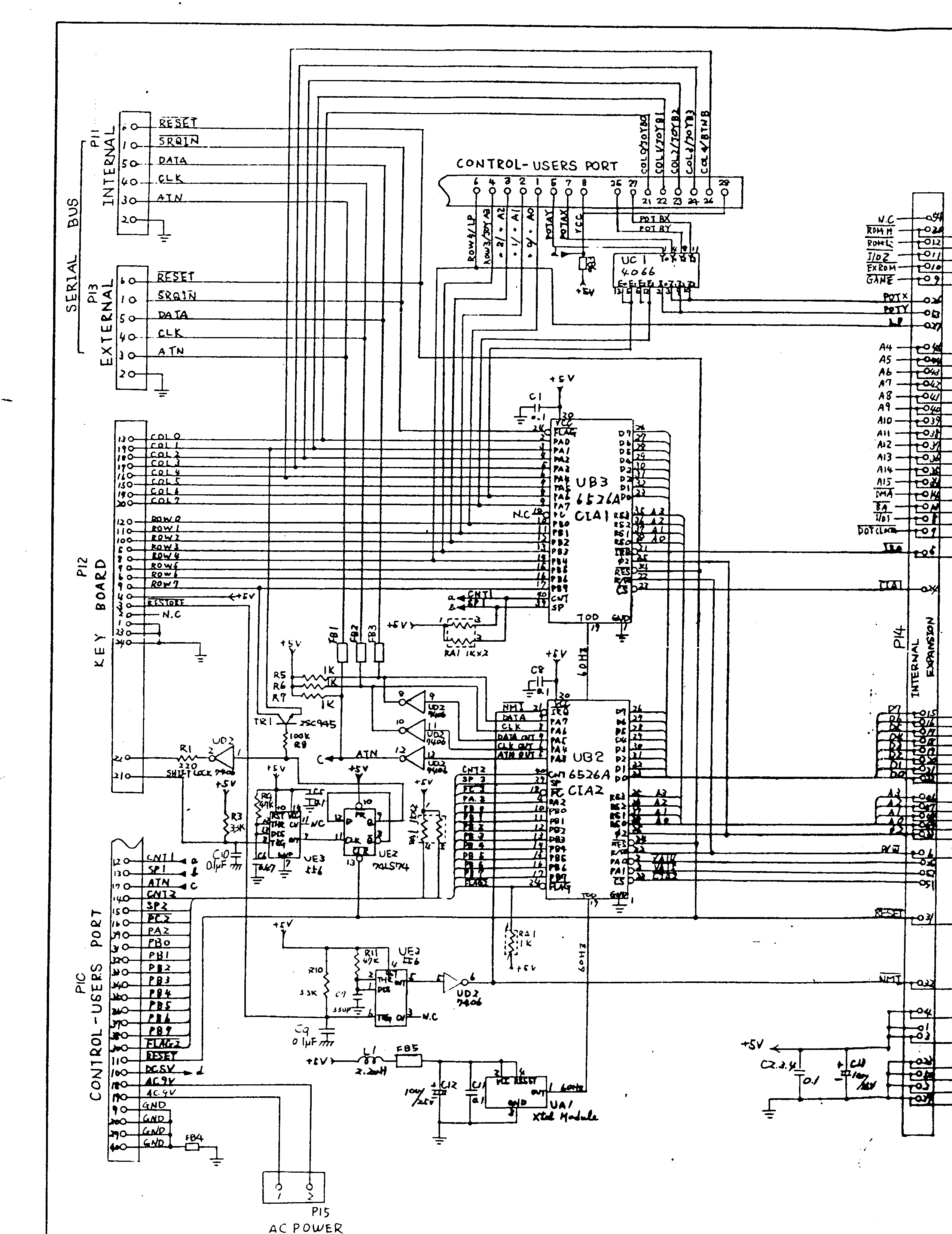
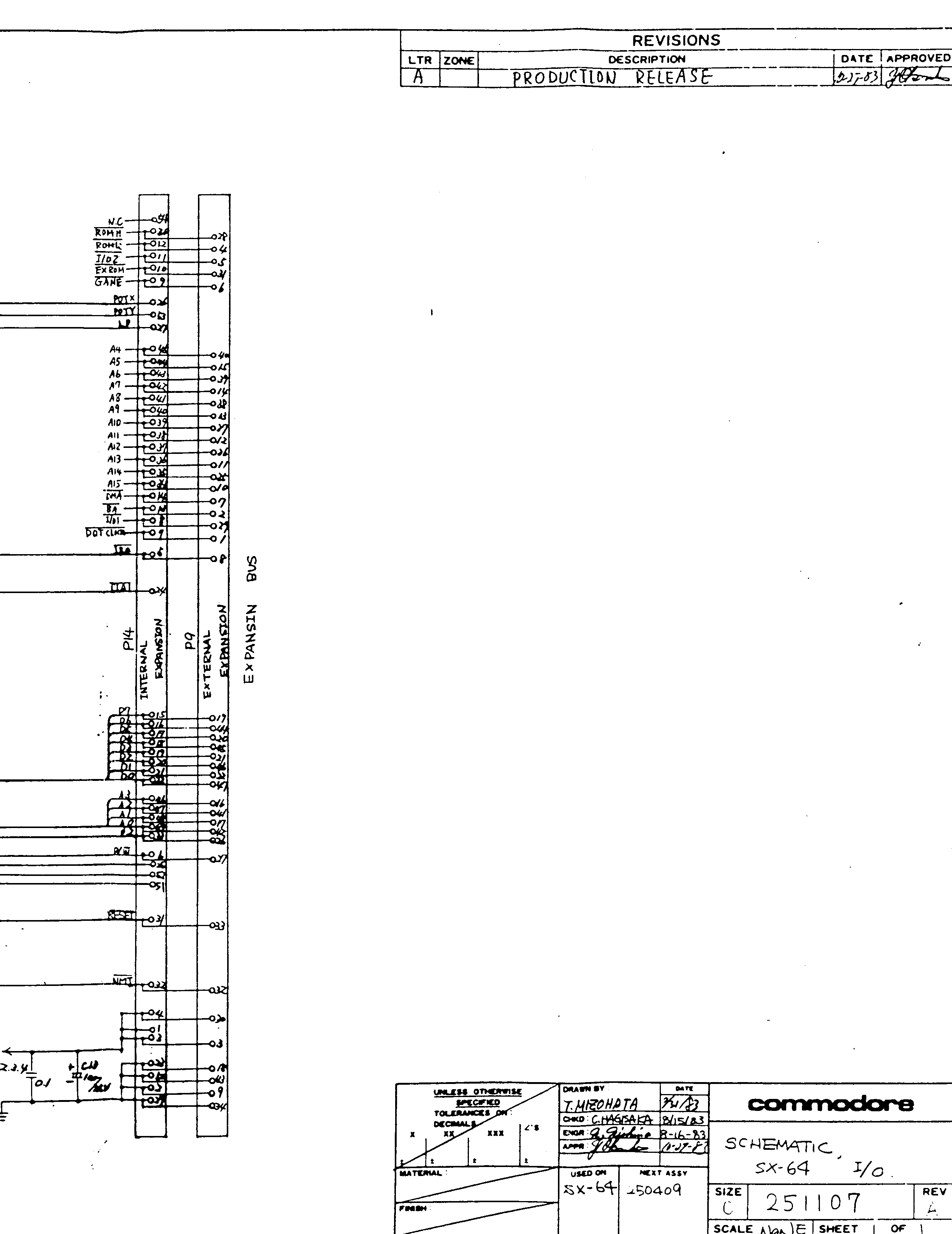
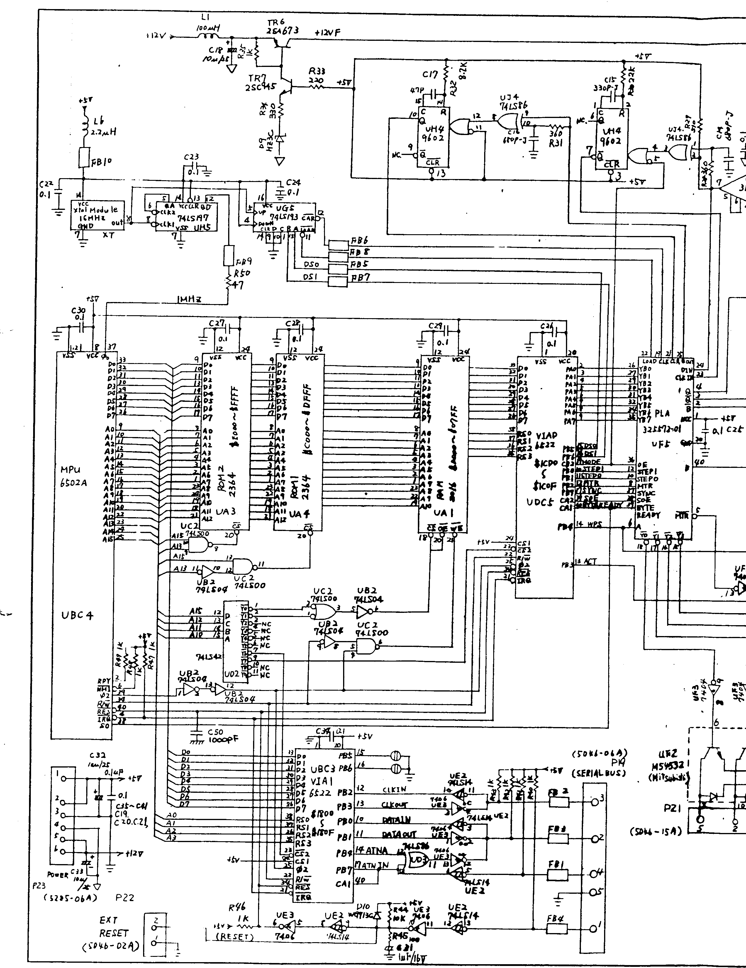
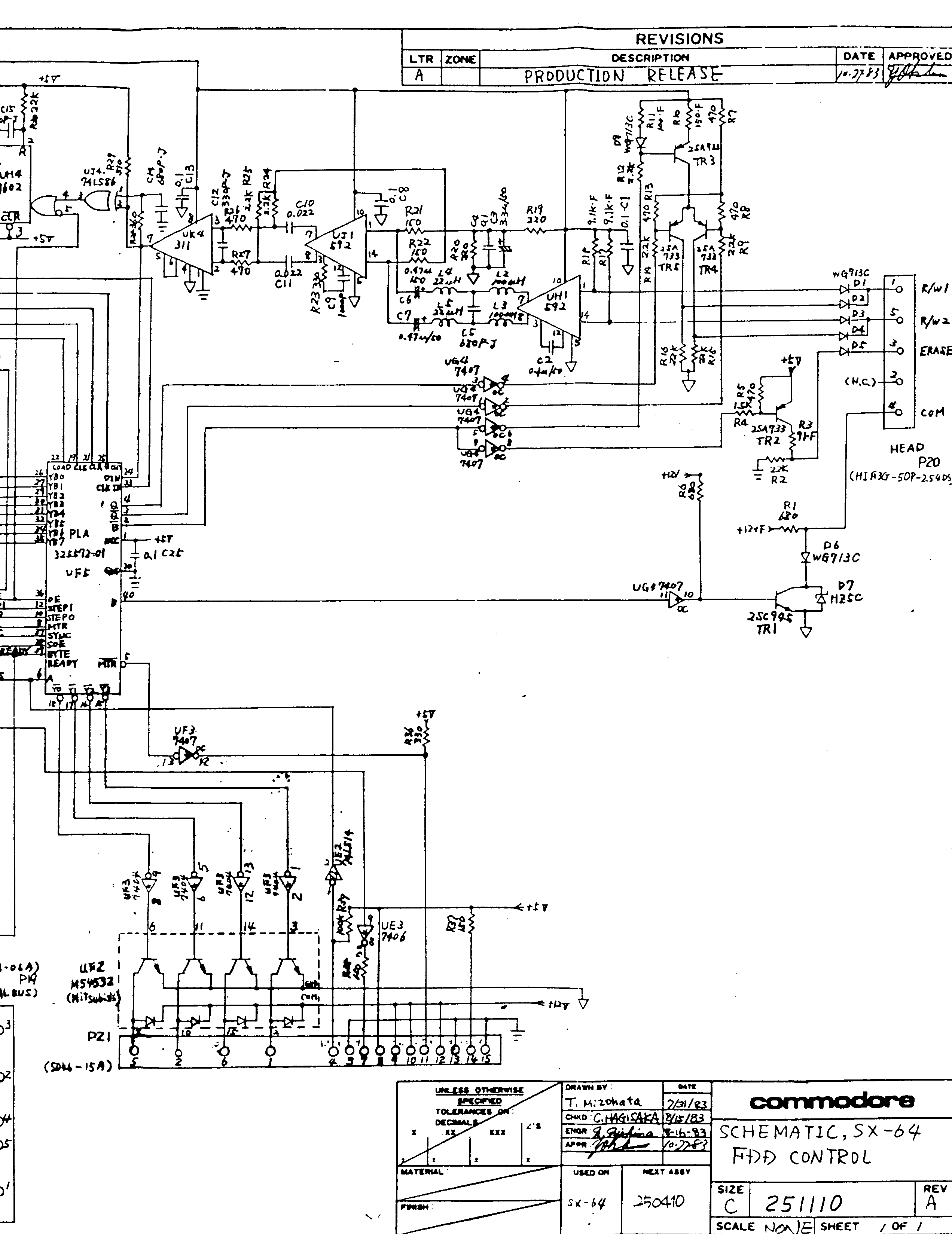
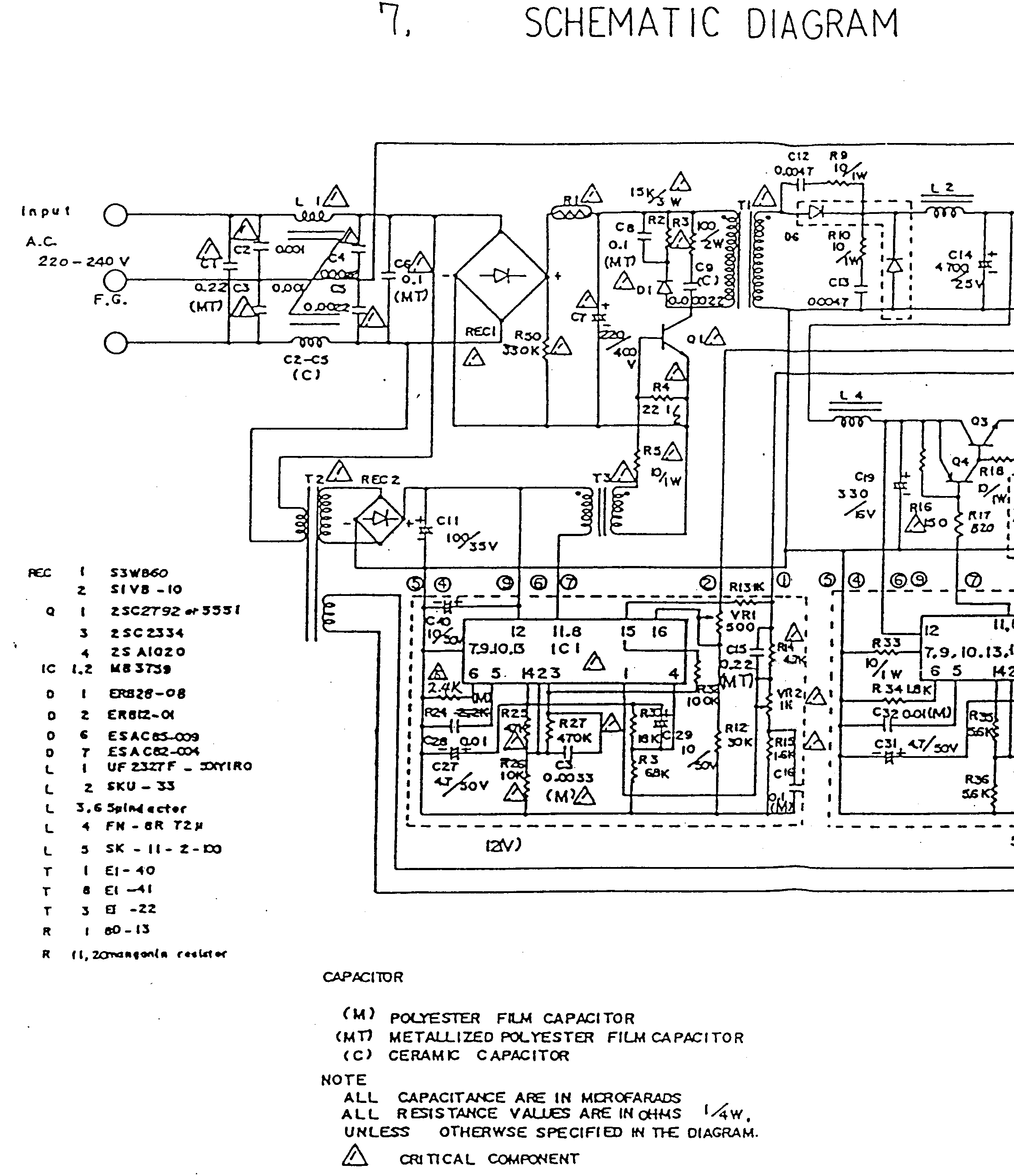
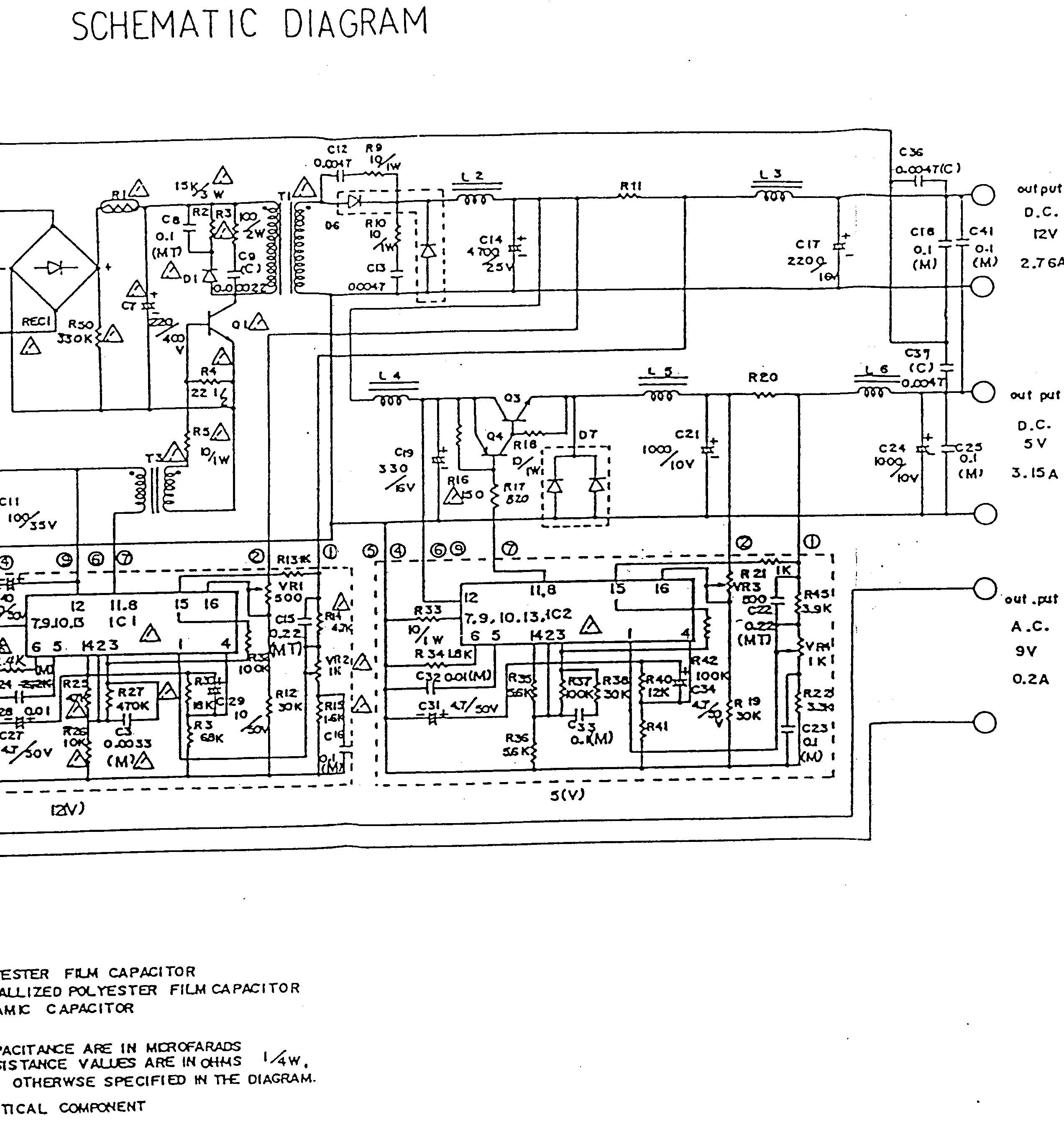
Miscellaneous SX64 schematics
The C1541 Service Manual in html format
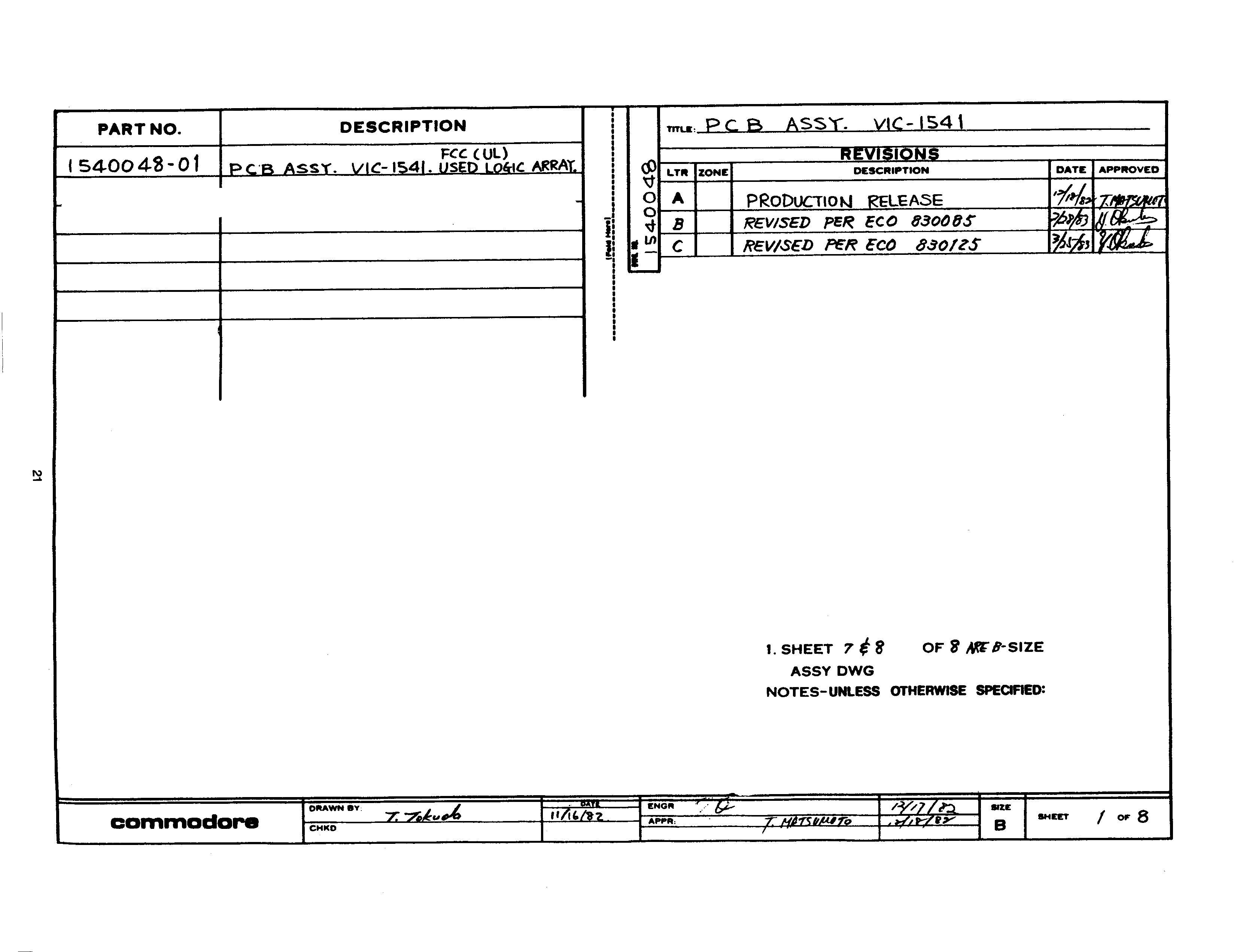
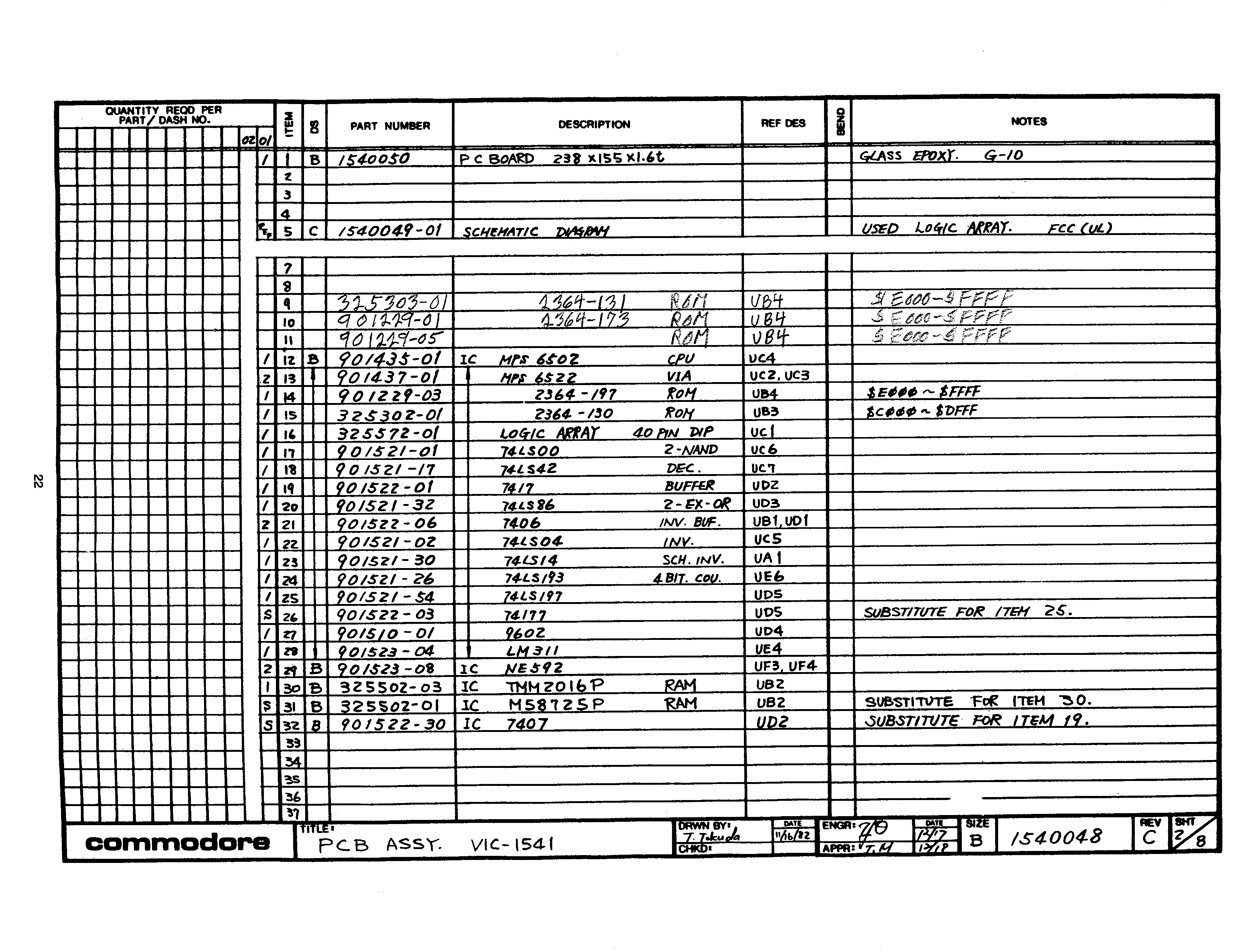
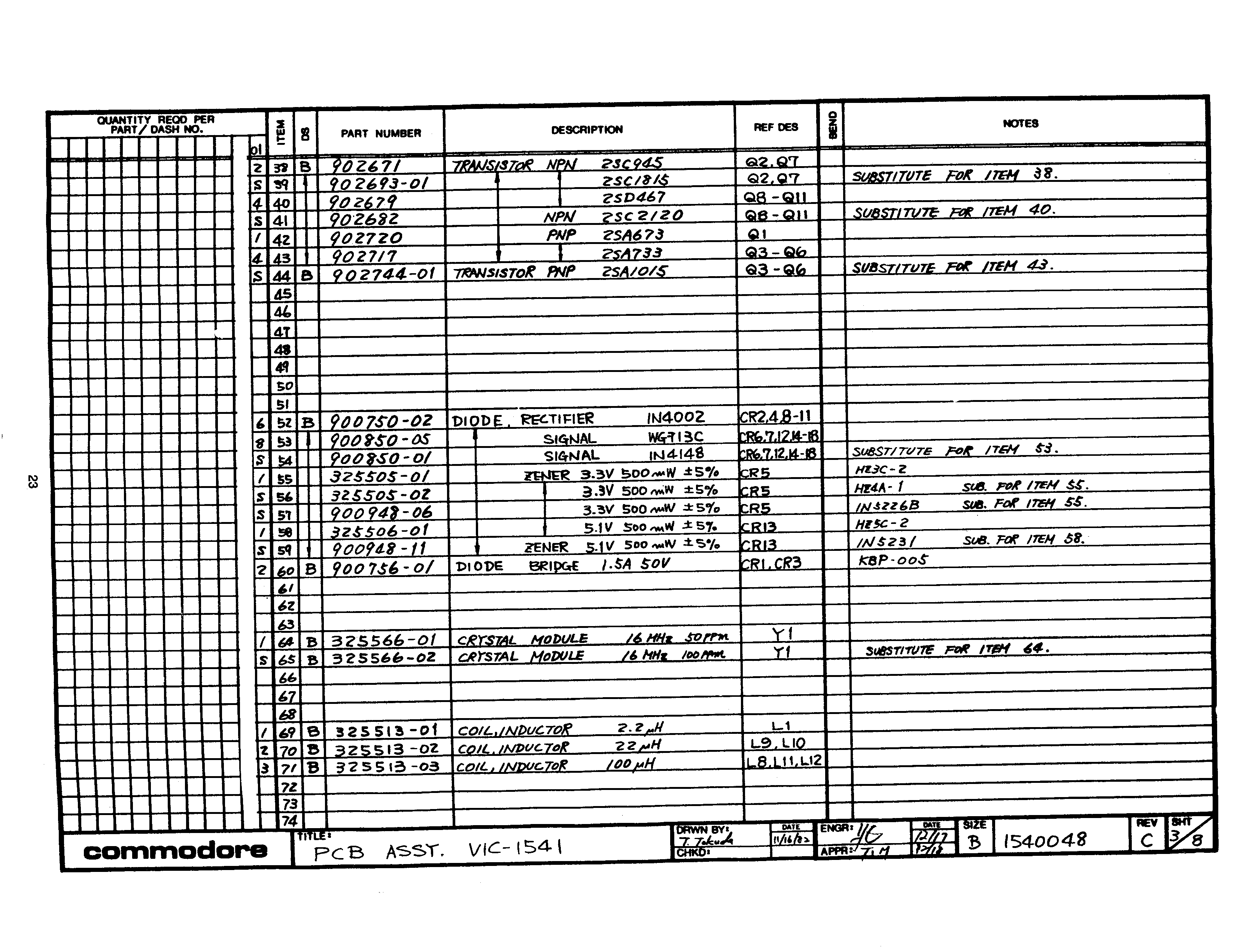
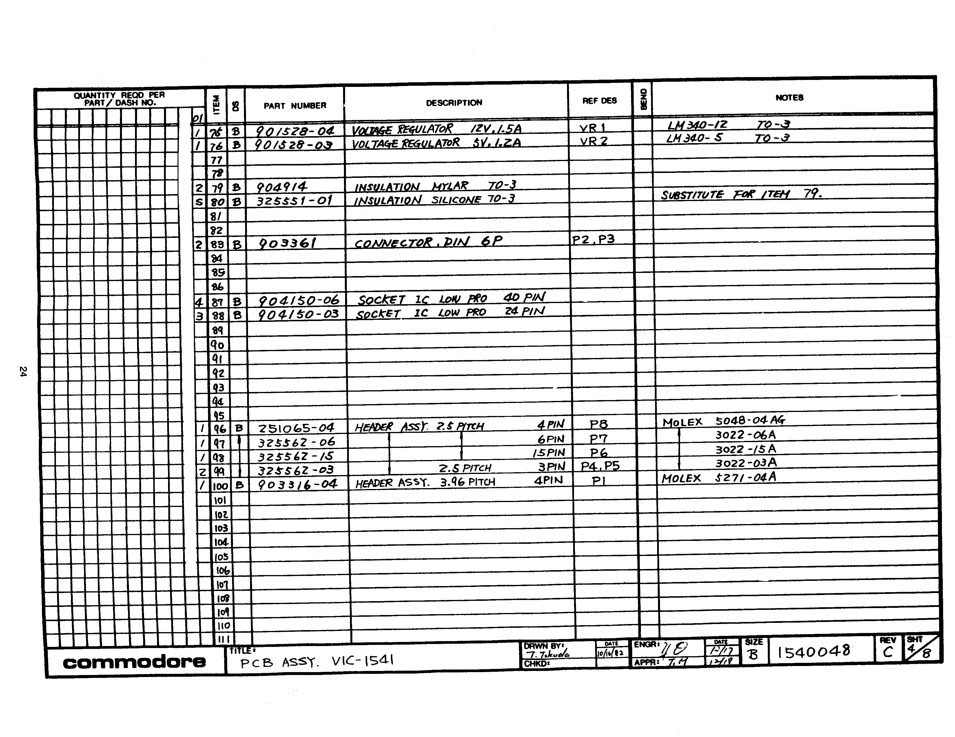
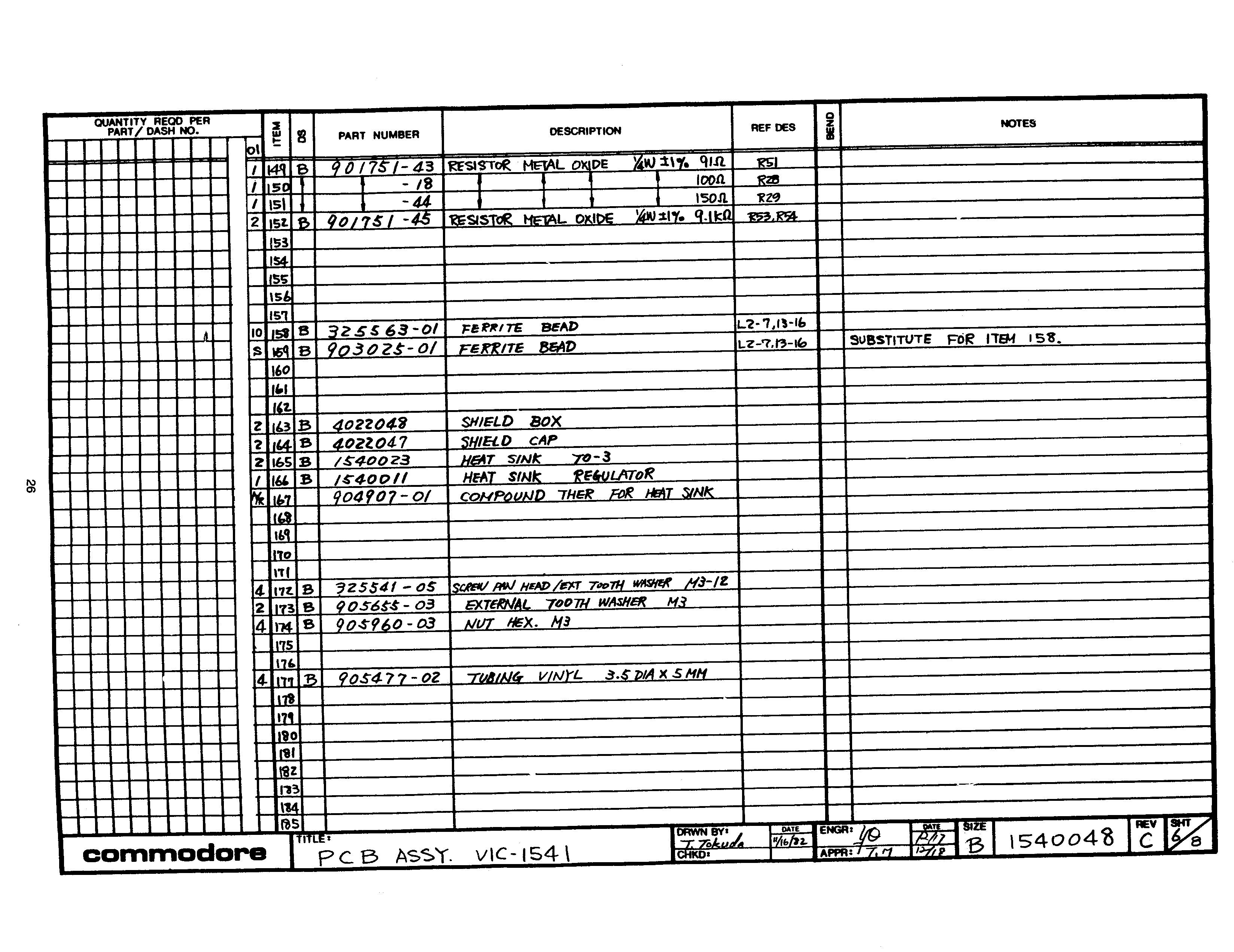
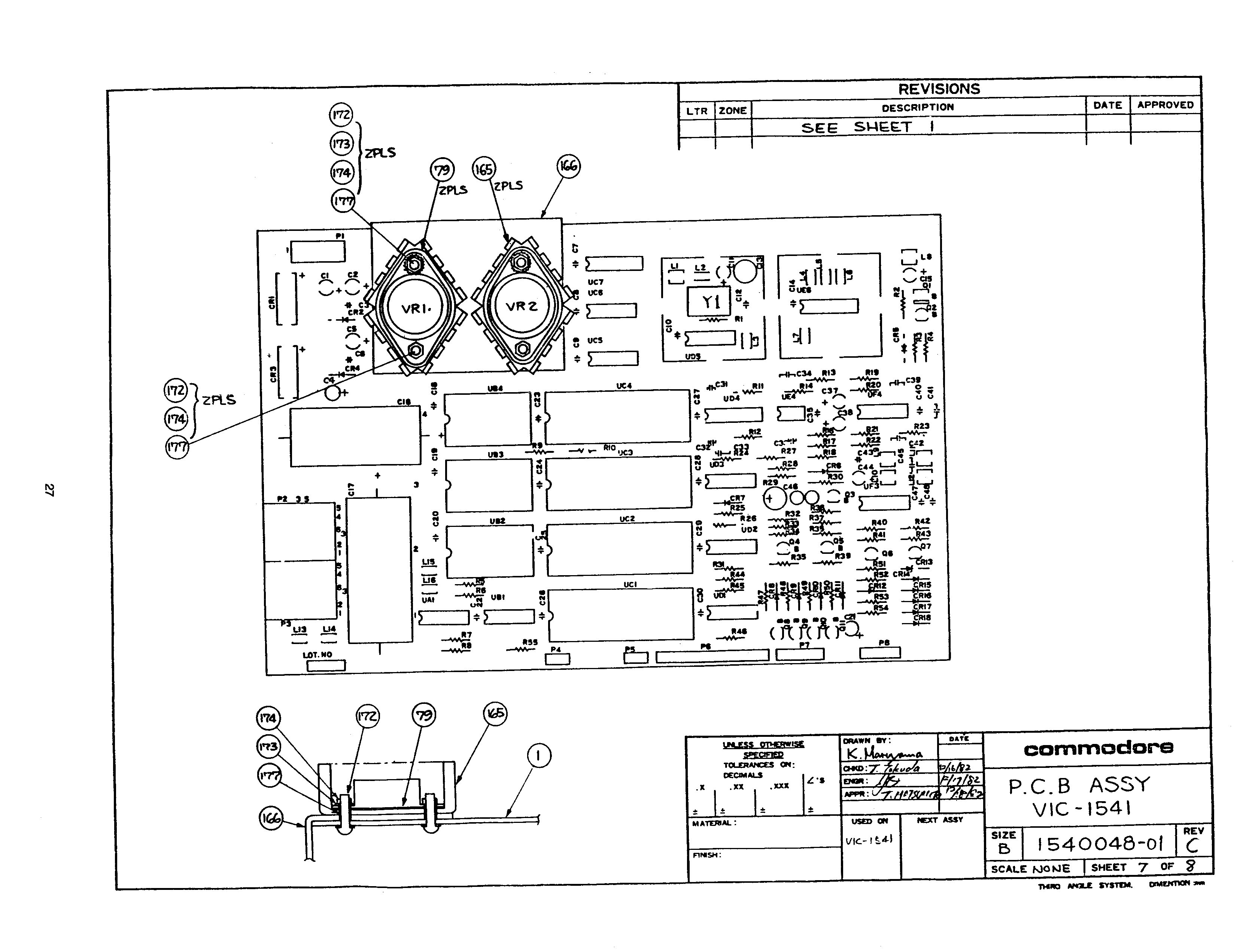
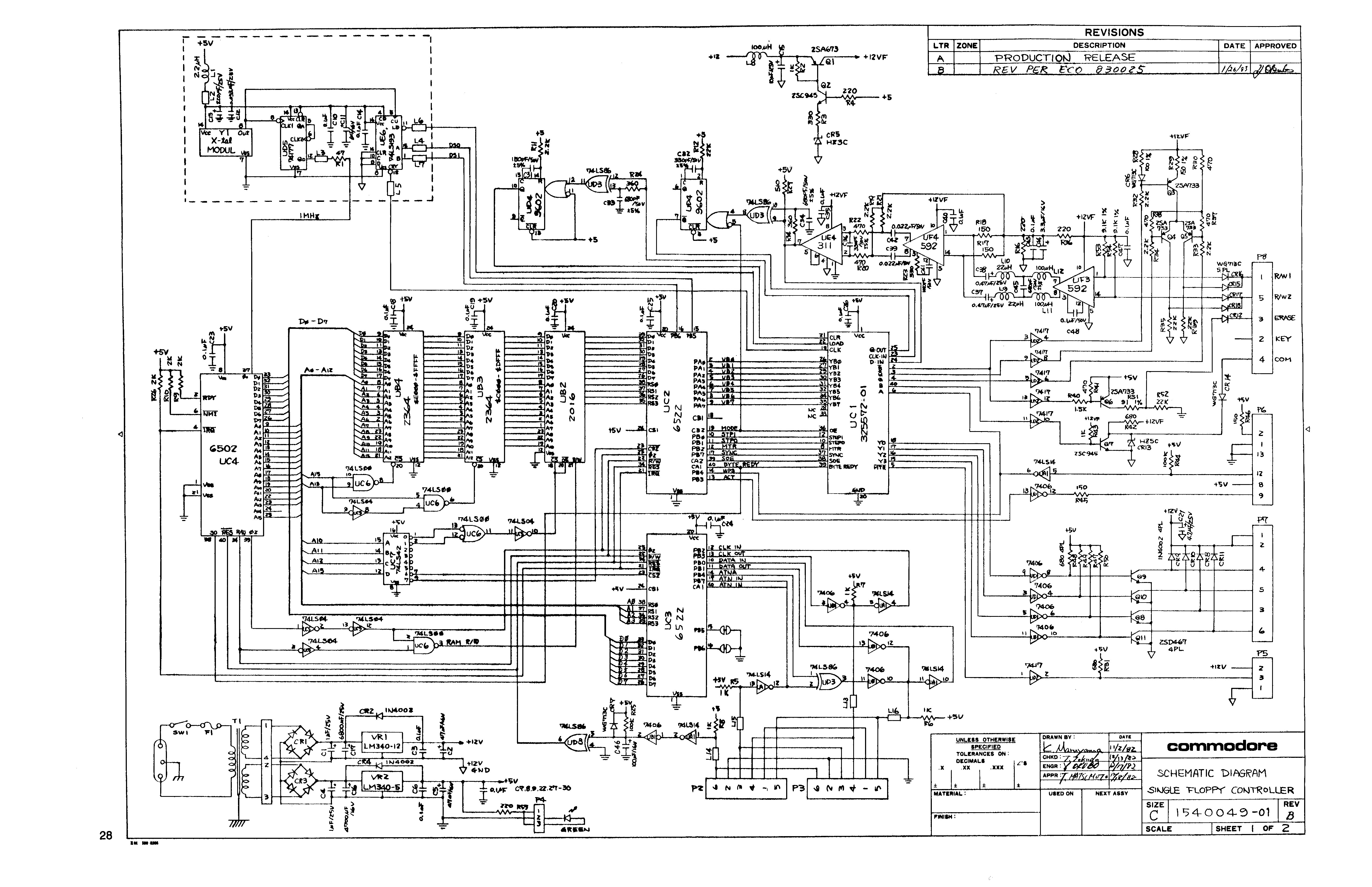
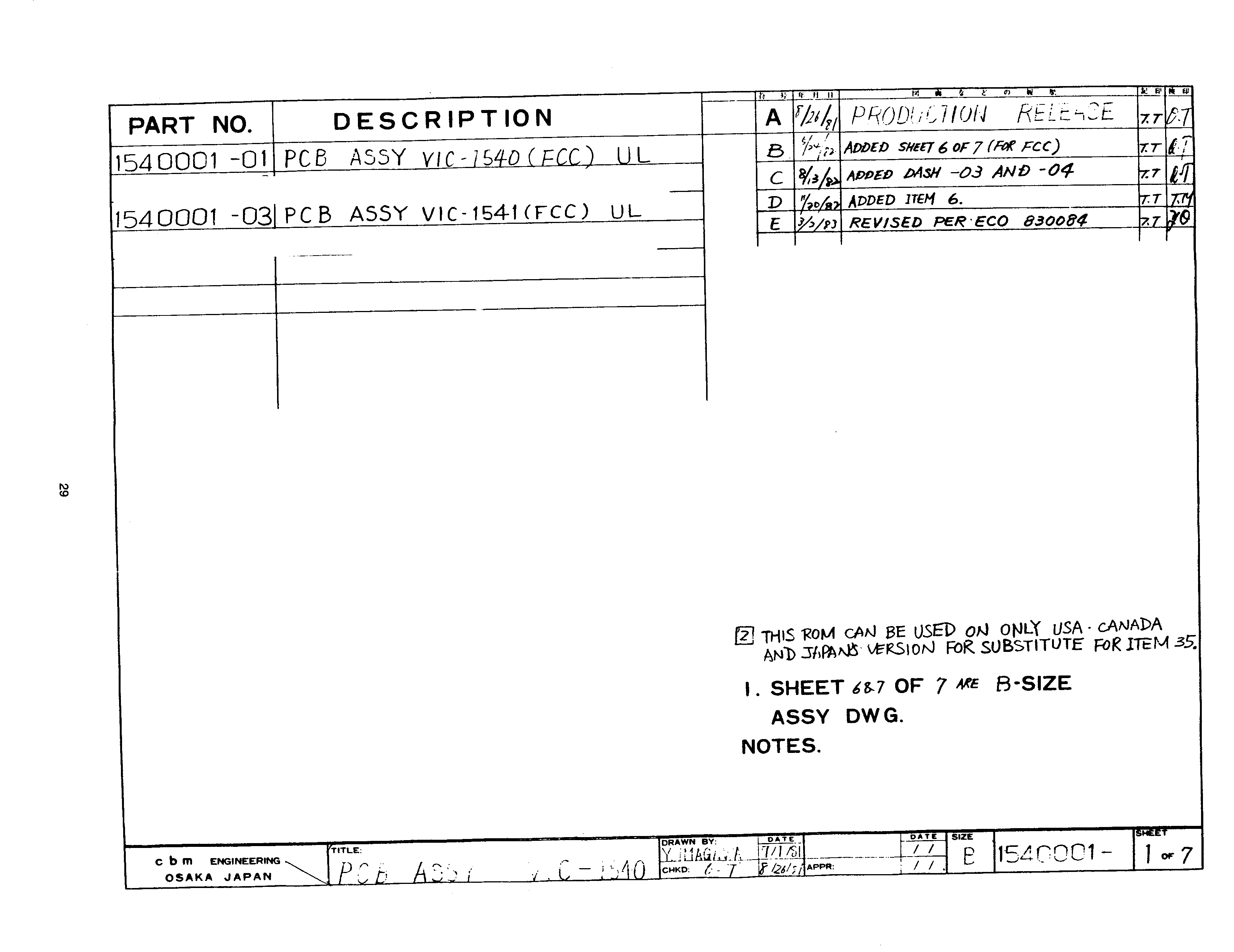
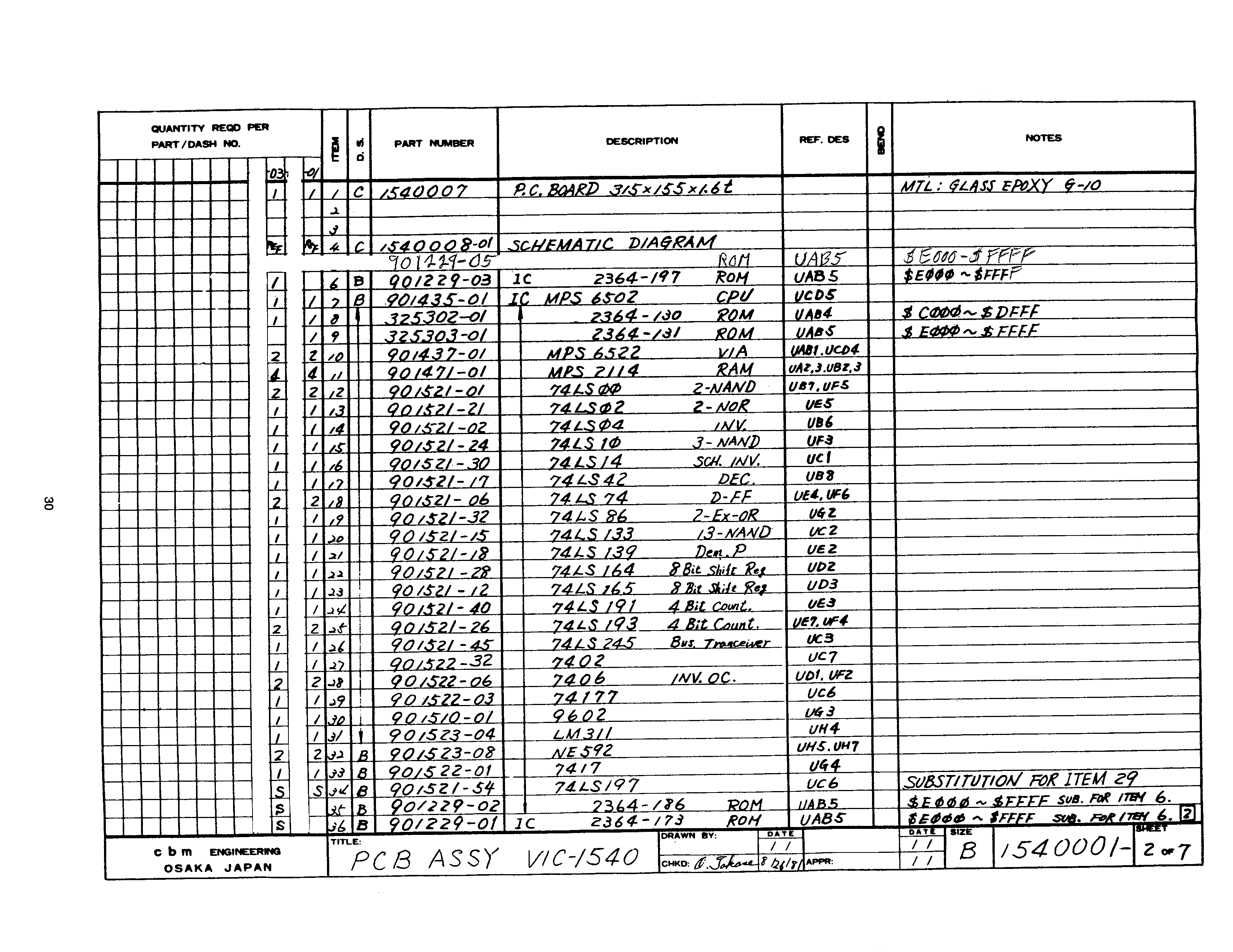
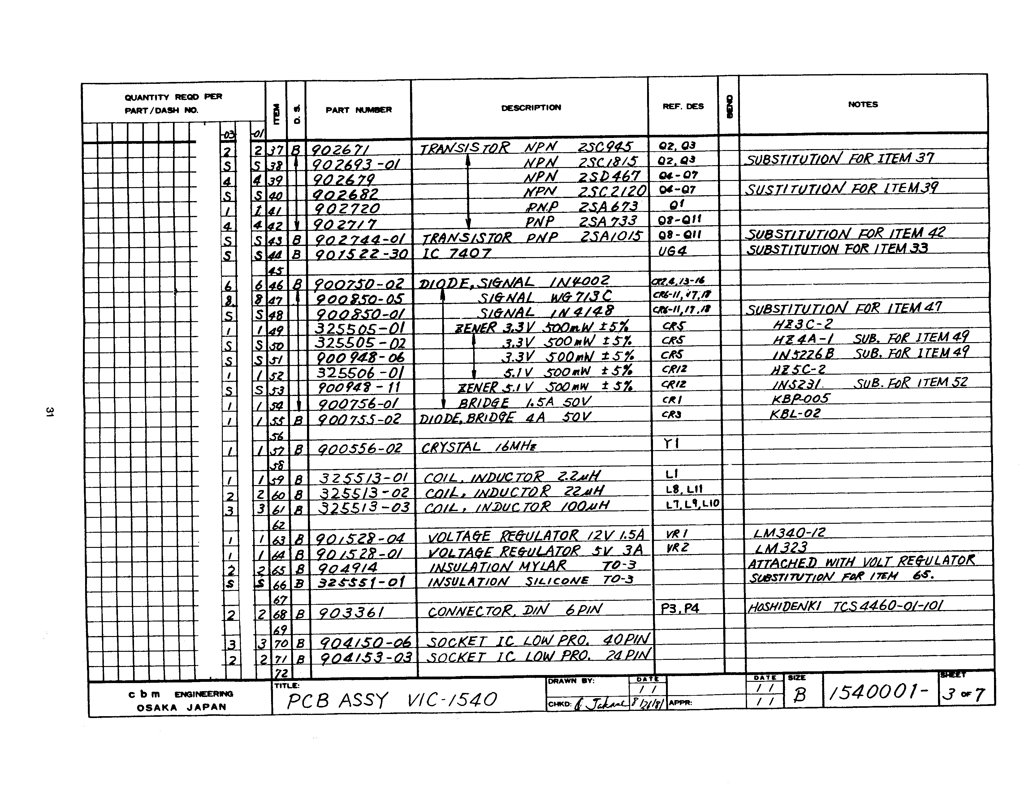
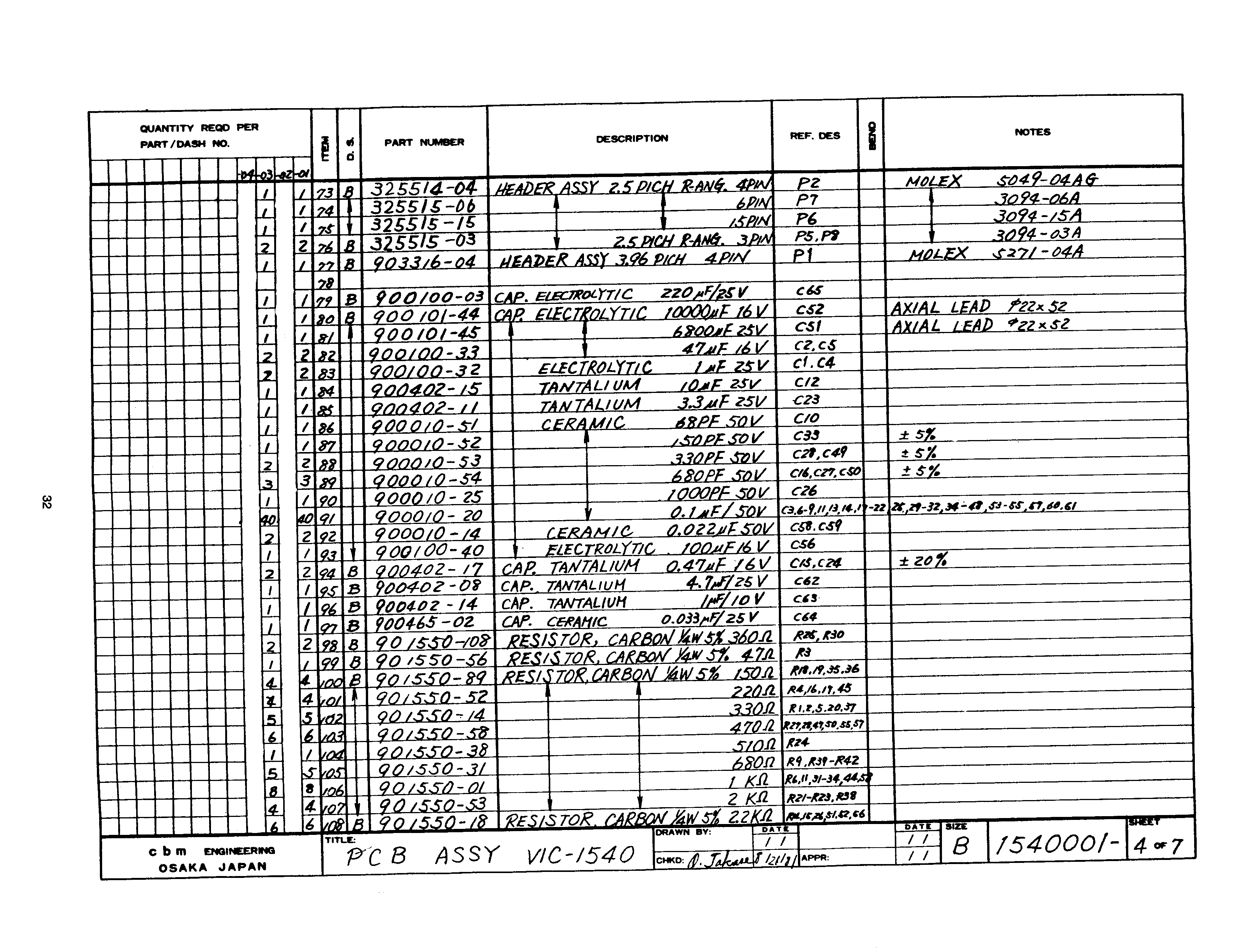
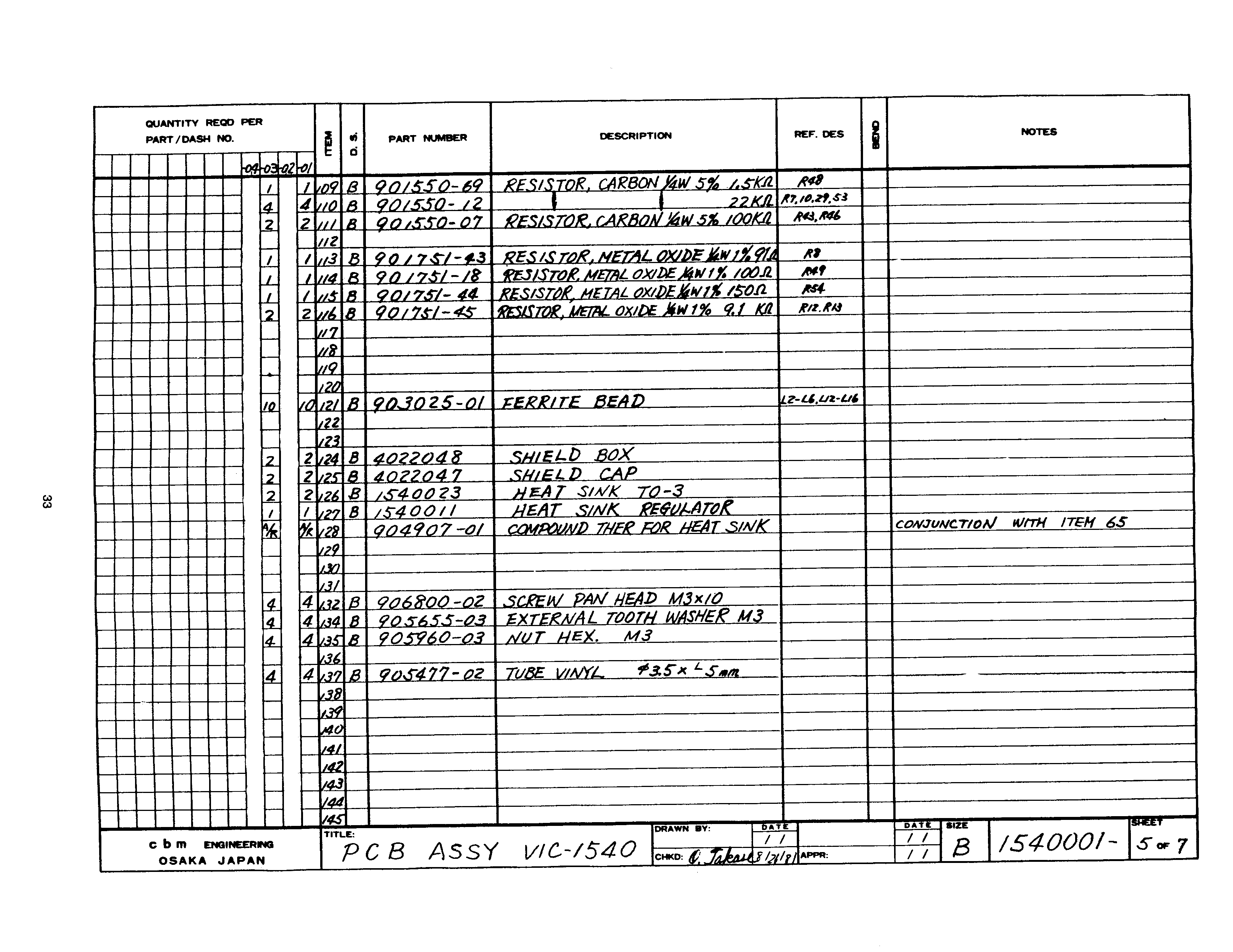
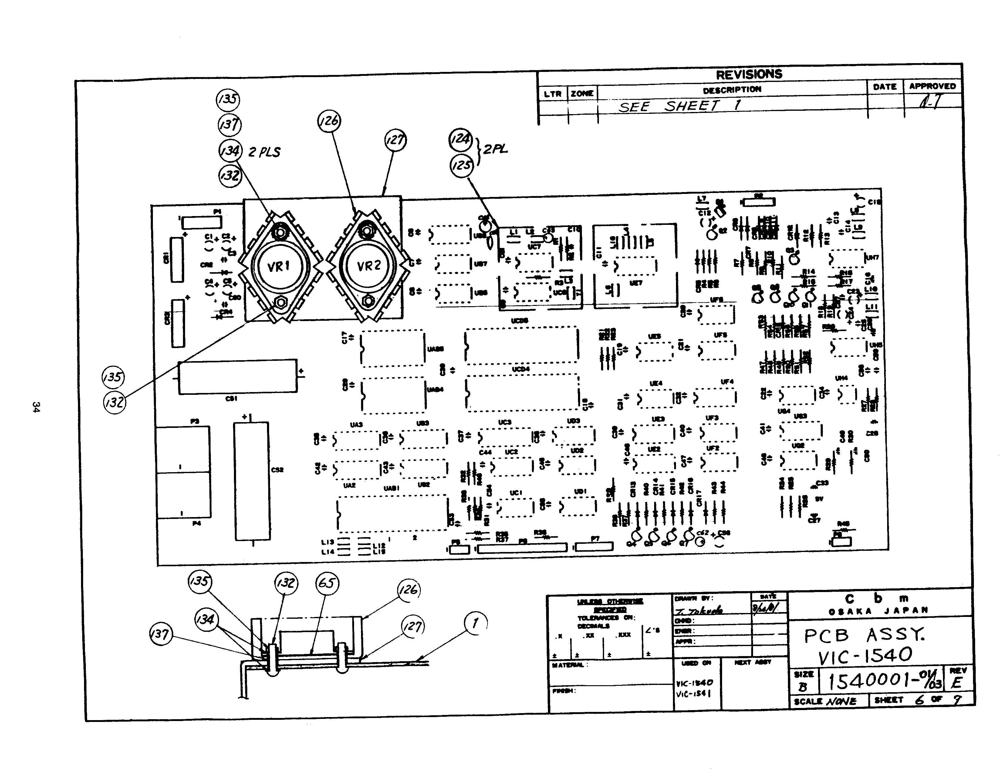
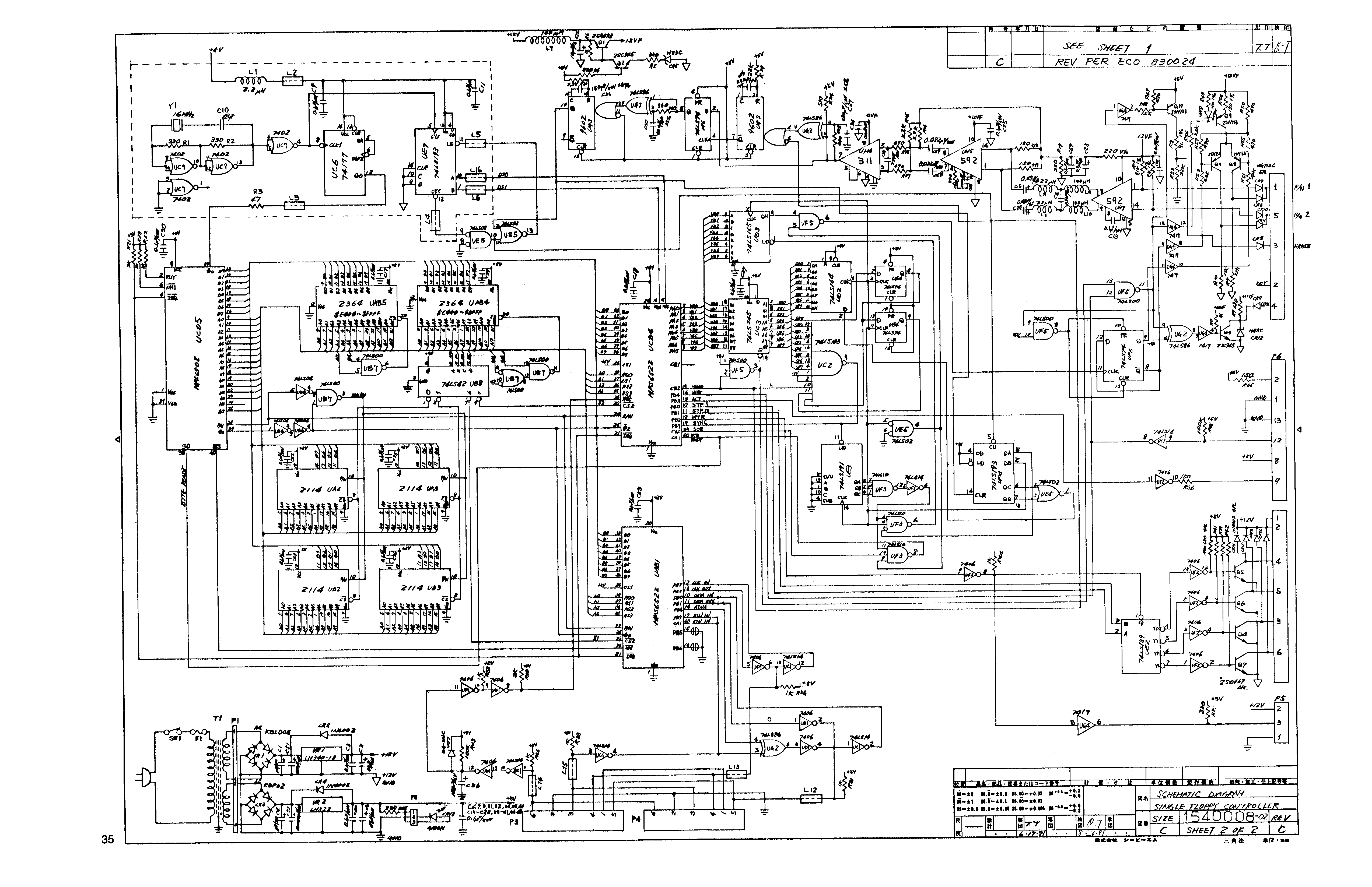
The scanned C1541 Technical Manual
- page:
title,
contents,
01,
02,
03,
04,
05,
06,
07,
08,
09,
10,
11,
12,
13,
14,
15,
16,
17,
18,
19,
20,
21,
22,
23,
24,
25,
26,
27,
28,
29,
30,
31,
32,
33,
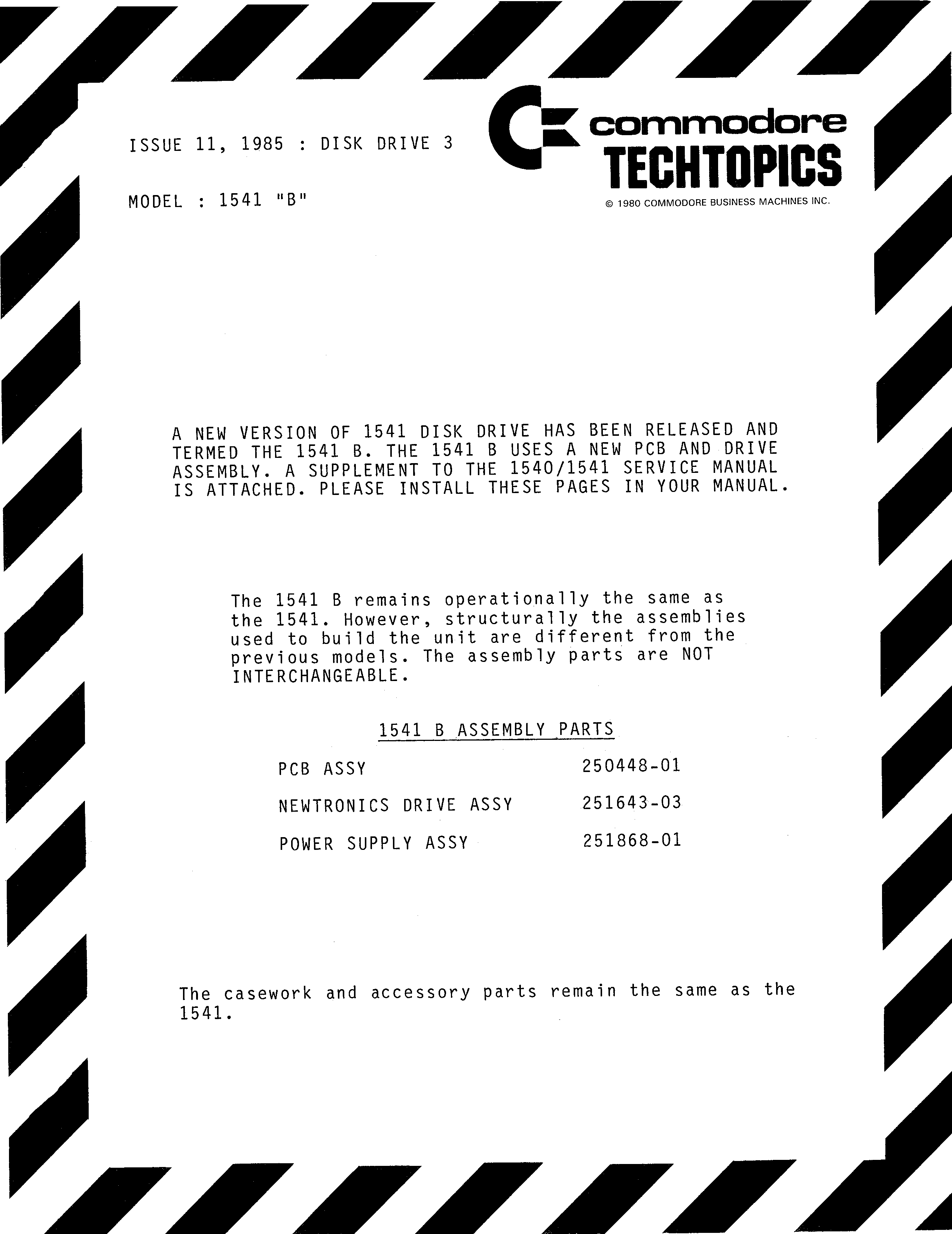
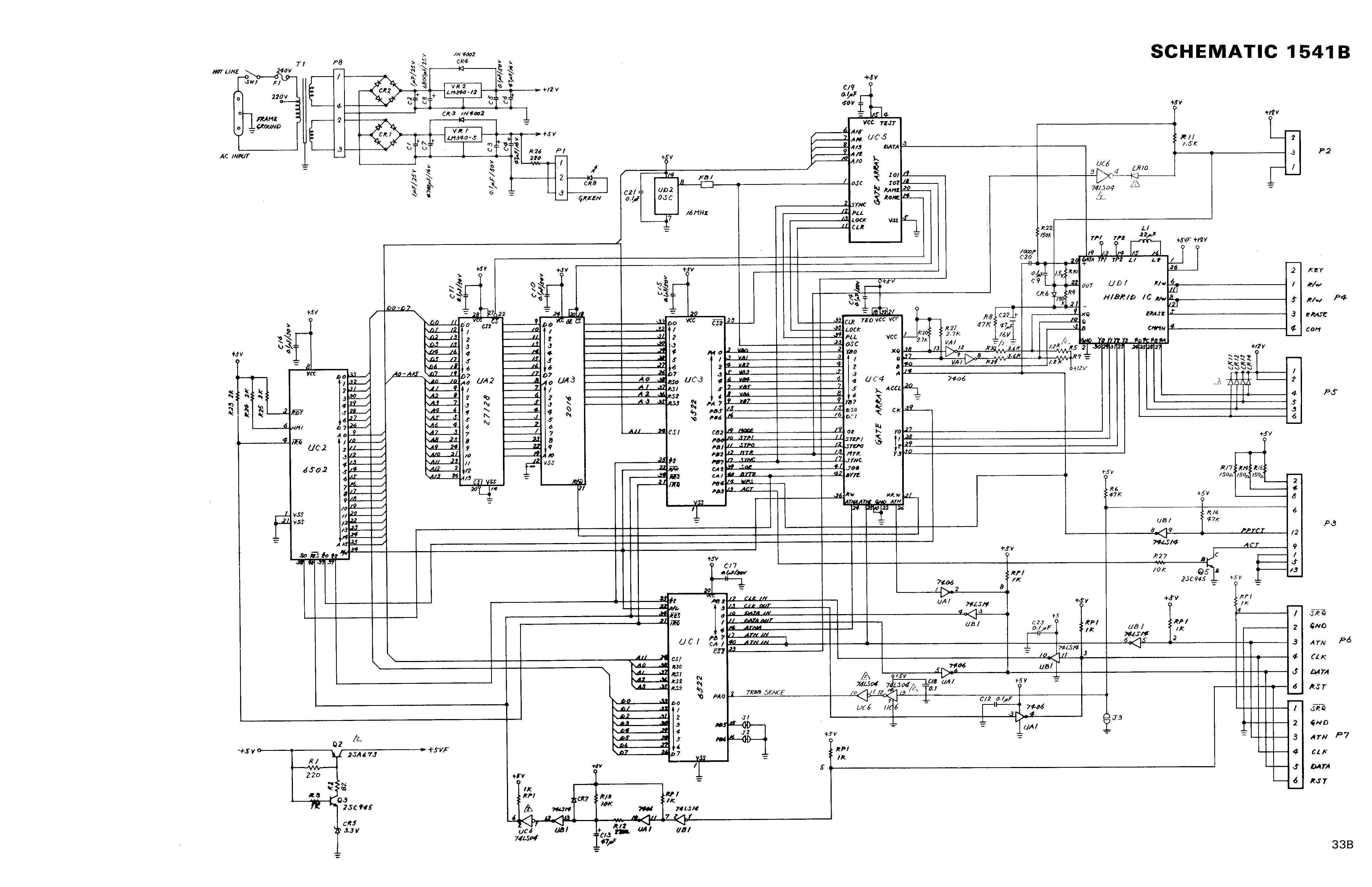
33ba,
33bb,
33bc,
33bd,
34,
35,
36,
37,
38,
39,
40
Miscellaneous C1541 schematics
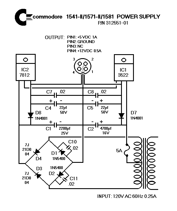
- Reverse-engineered schematic diagram of the 110-volt 1581 and 1541-II
power supply. Created and uploaded by William Levak.
According to him, you have to break the case open to get inside. Jameco
sells a case that can be used to replace it.
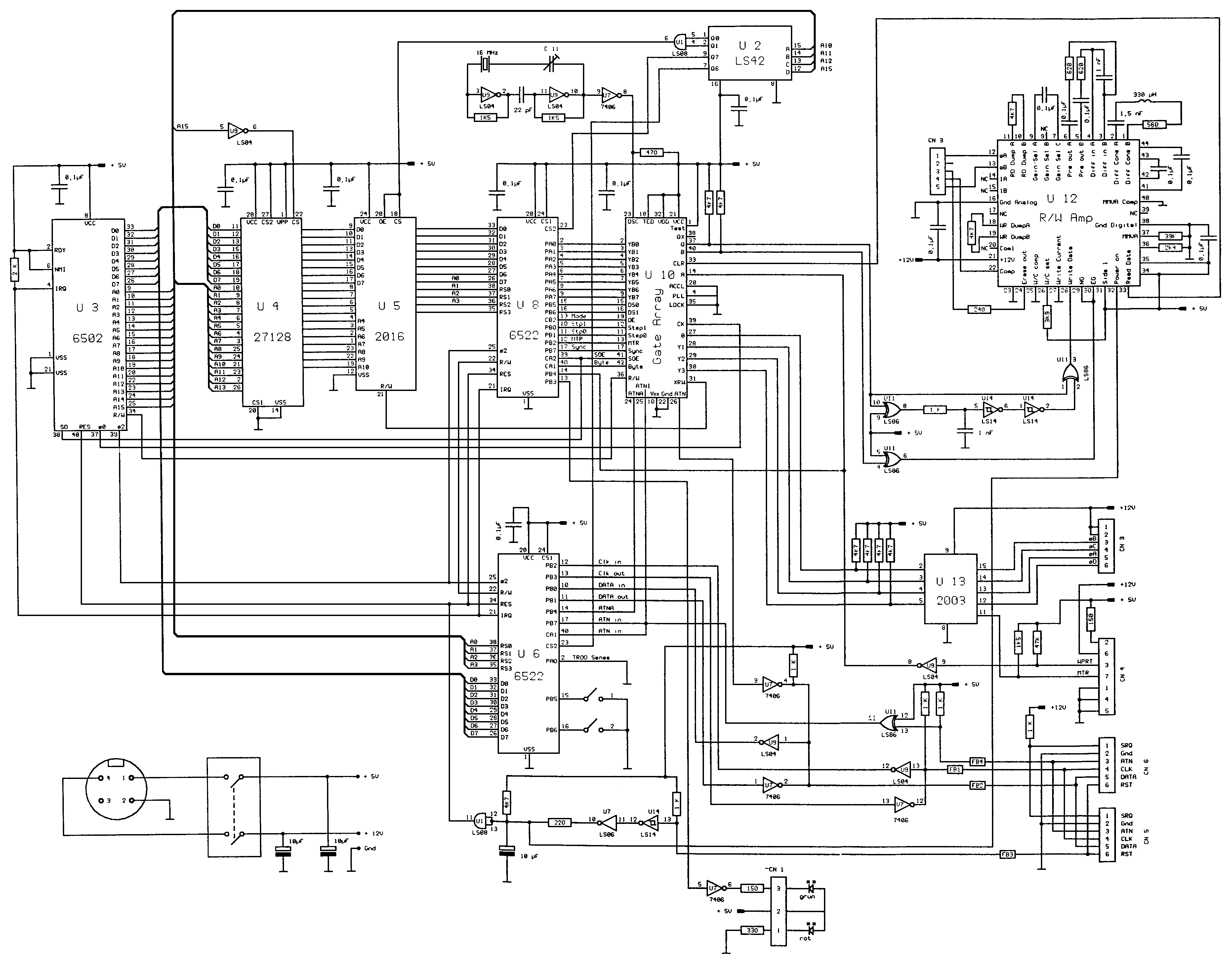
- 1541-II schematic diagram, by Commodore. According to the 1571 Service
Manual, the Gate Array (251828 or 64H156) has some different revisions
(-01, -02 and -03). Revisions -01 and -03 have only 40 pins, but -02 has
42 pins. Frank Kontros reports that the (chinese)
1541-II boards he has seen only carry the assy no. 340503, although there
are some differences. Also, his boards have the latest (-03) Gate Array,
with some wiring on the pin 21 (OSC).
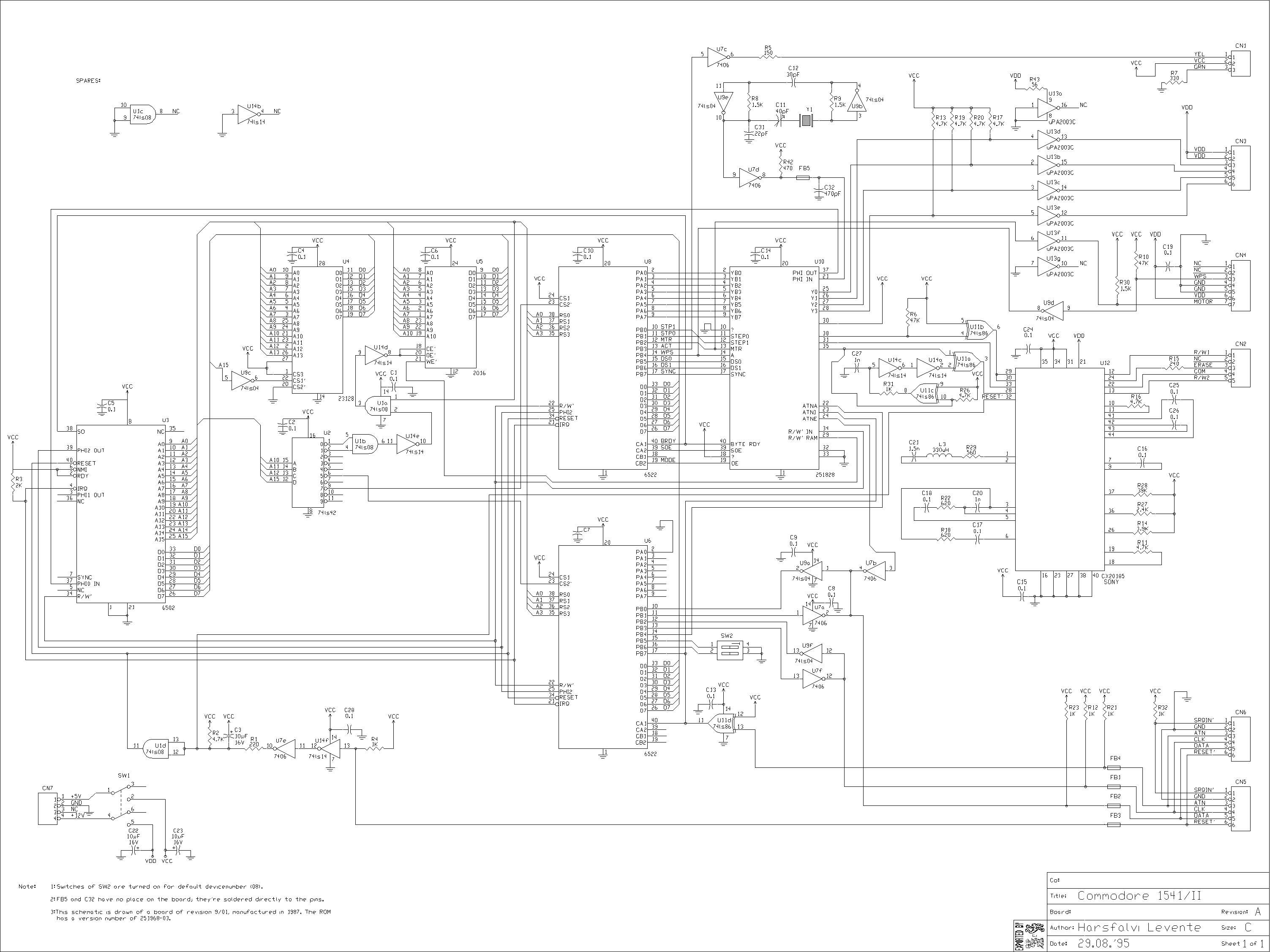
- 1541-II schematic diagram. Drawn by
Levente Harsfalvi. See also the note
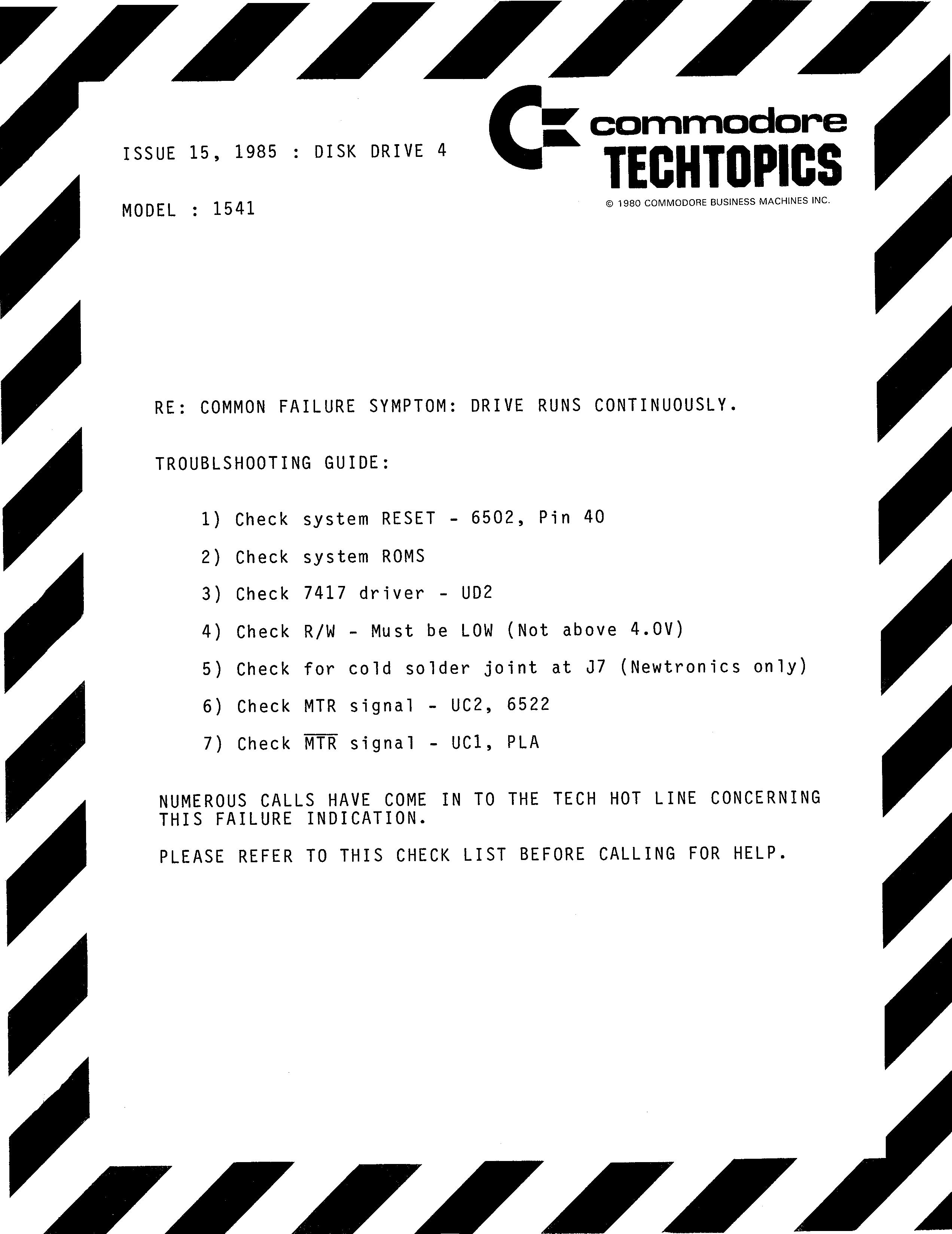
- Information about different 1541 board versions, composed by William Levak.
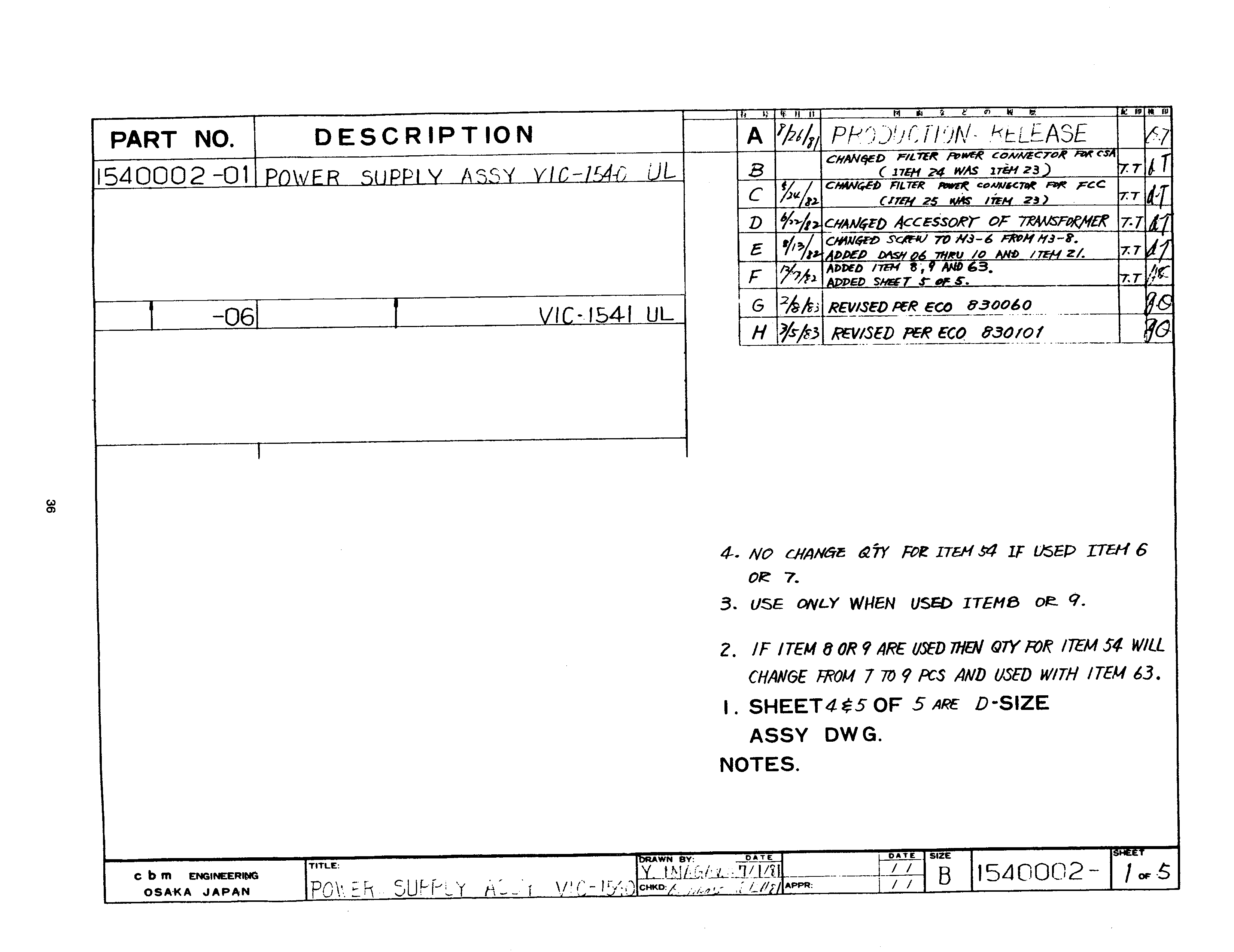
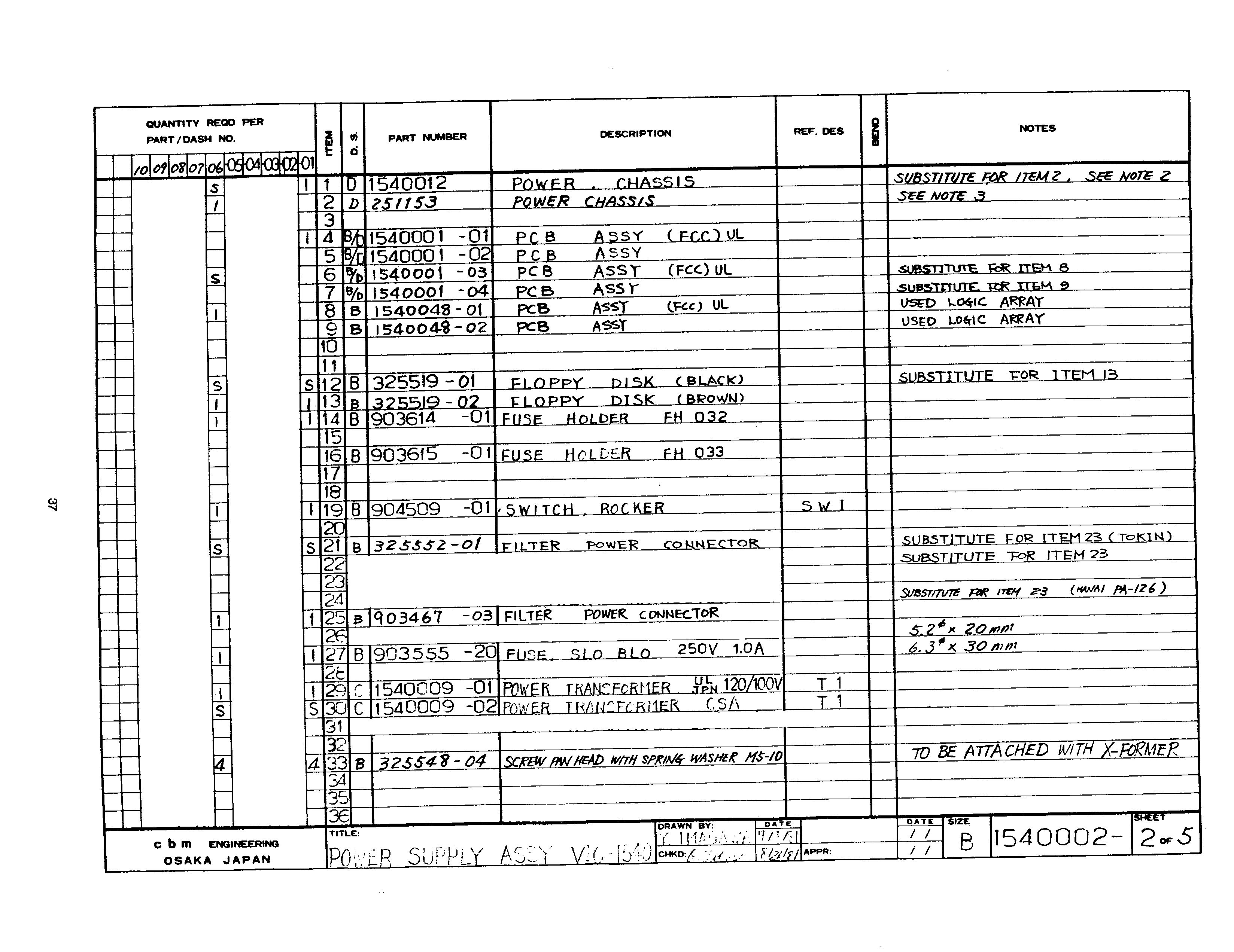
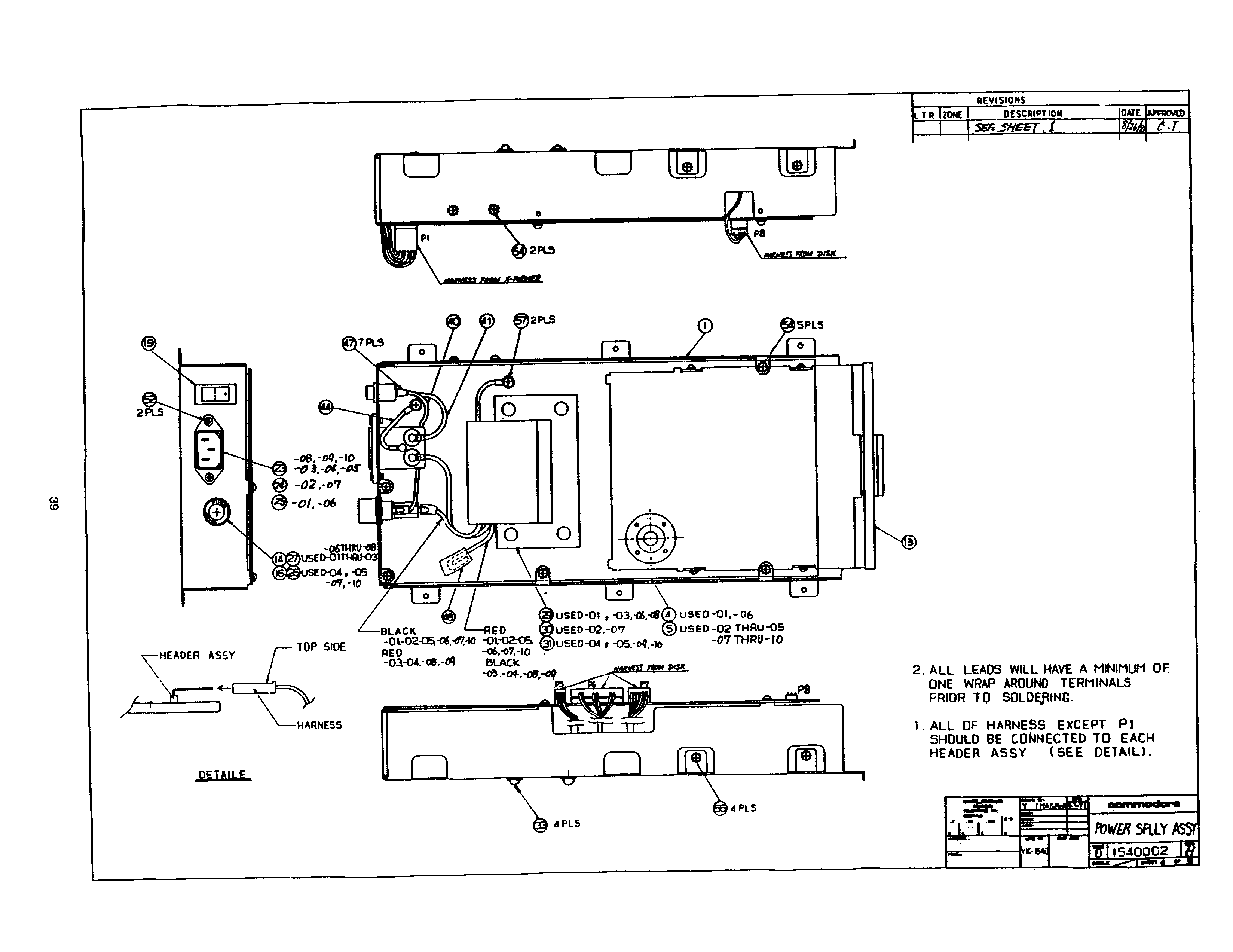
- 1540/1541/1541A/SX-64 drive parts list, composed by William Levak.
- 1541/1571 40/42 Pin Gate Arrays, composed by William Levak.
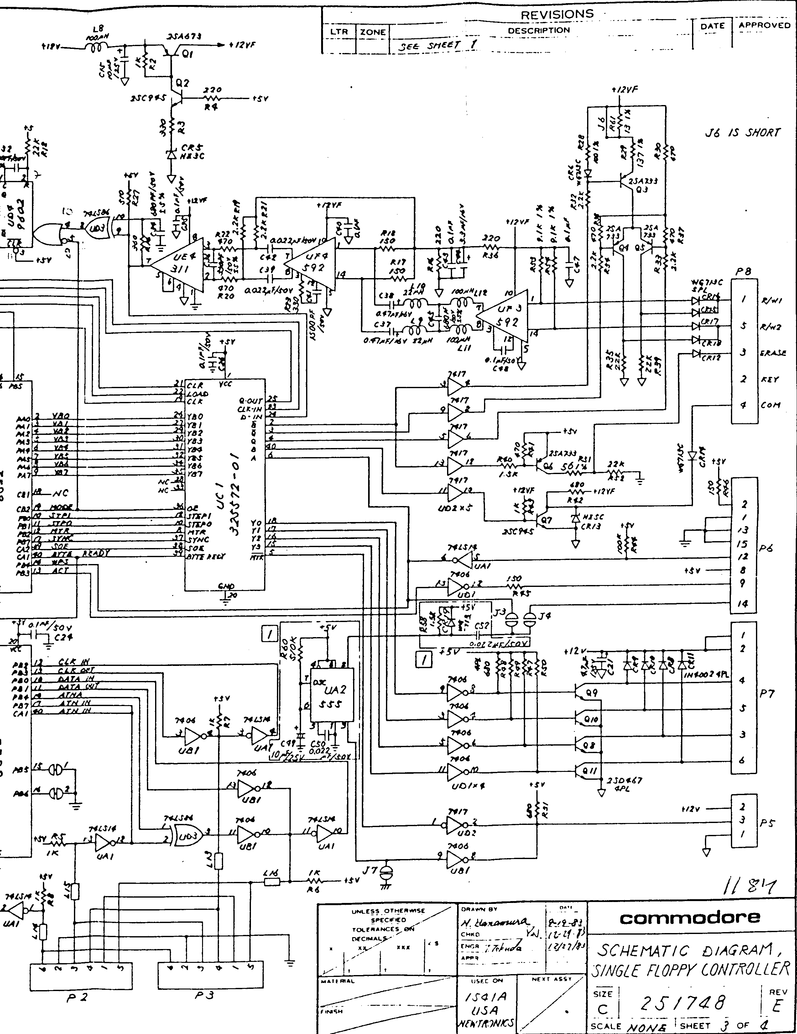
- 251748-E-left,
251748-E-right:
Short board 1541, assy no. 251748, rev.E, sheet 3 of 4. On this board, a
40-pin custom chip replaces some 74xx logic.
Some more technical information
|